

Aston在下不求
1.2k Posts

Aston在下不求
Report
Block User
I post critical crypto market data and my most reliable trade signals—always with charts & real examples. 關注我將不定期得到幣圈總體經濟數據重要數據,也將把我勝率高的進場出場點位告訴大家有圖有實盤。

BNB Holder
High-Frequency Trader
8.1 Years
888 Following
21.4K+ Followers
4.7K+ Liked
Posts
All
Quotes
Videos
Live
PINNED
·
--
【Exclusive Benefits for Public Copy Trading】90-Day Capital Protection Plan + Taiwan-Exclusive Gifts 🎁
Hello, friends in Taiwan! I’m promoting my “public copy trading” service. Just start copy trading and send me a screenshot in a private message, and I’ll not only help you trade steadily, but also send you an exclusive physical gift!
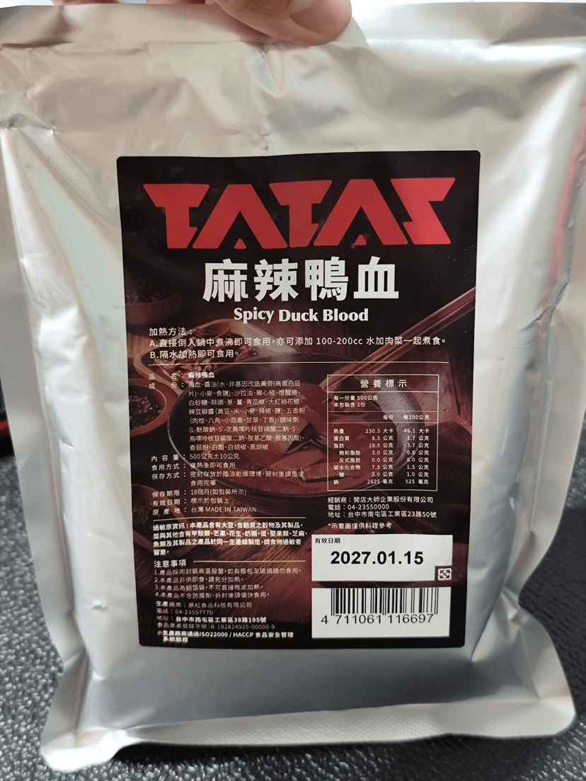
🍲 Copy-Trading Gift (shipped within three months): “Spicy Duck Blood Hot Pot Meal Kit”! Net weight: 500 grams. Packaging: aluminum foil pouch.
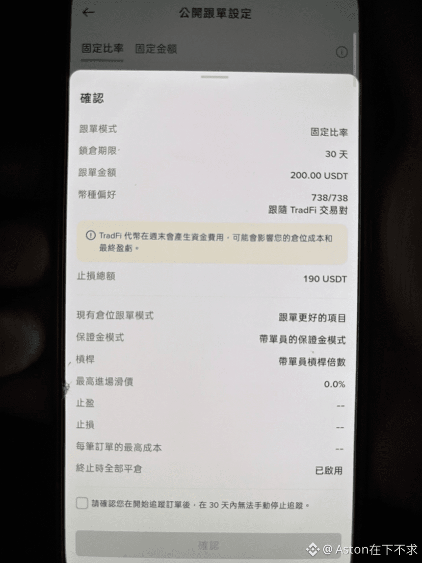
⚙️ Required Copy-Trading Settings (please copy exactly):
Mode: #定比跟单
Stop loss: None
Margin: Follow the lead trader’s mode
Leverage: Follow the lead trader’s leverage
Trading pairs: Follow TridFi trading pairs #TridFi晒单
🛡️ 90-Day Capital Protection Guarantee #保本盈利 : If you copy trade in the “public” group for more than 90 days and your final settlement shows no profit, I’ll reimburse your losses in full!
⚠️ Please note:
This offer is open to all regions, but applies only to “public copy trading.” Private copy trading is not covered by the capital protection guarantee.
The maximum protected amount is $1,000. (If your copy-trading principal exceeds $1,000, the excess is not guaranteed to be fully reimbursed.)
If you have any questions about copy trading or the settings, feel free to join my chatroom and ask anytime!
【Exclusive Benefits for Public Copy Trading】90-Day Capital Protection Plan + Taiwan-Exclusive Gifts 🎁
Hello, friends in Taiwan! I’m promoting my “public copy trading” service. Just start copy trading and send me a screenshot in a private message, and I’ll not only help you trade steadily, but also send you an exclusive physical gift!
🍲 Copy-Trading Gift (shipped within three months): “Spicy Duck Blood Hot Pot Meal Kit”! Net weight: 500 grams. Packaging: aluminum foil pouch.
⚙️ Required Copy-Trading Settings (please copy exactly):
Mode: #定比跟单
Stop loss: None
Margin: Follow the lead trader’s mode
Leverage: Follow the lead trader’s leverage
Trading pairs: Follow TridFi trading pairs #TridFi晒单
🛡️ 90-Day Capital Protection Guarantee #保本盈利 : If you copy trade in the “public” group for more than 90 days and your final settlement shows no profit, I’ll reimburse your losses in full!
⚠️ Please note:
This offer is open to all regions, but applies only to “public copy trading.” Private copy trading is not covered by the capital protection guarantee.
The maximum protected amount is $1,000. (If your copy-trading principal exceeds $1,000, the excess is not guaranteed to be fully reimbursed.)
If you have any questions about copy trading or the settings, feel free to join my chatroom and ask anytime!
Hello, friends in Taiwan! I’m promoting my “public copy trading” service. Just start copy trading and send me a screenshot in a private message, and I’ll not only help you trade steadily, but also send you an exclusive physical gift!
🍲 Copy-Trading Gift (shipped within three months): “Spicy Duck Blood Hot Pot Meal Kit”! Net weight: 500 grams. Packaging: aluminum foil pouch.
⚙️ Required Copy-Trading Settings (please copy exactly):
Mode: #定比跟单
Stop loss: None
Margin: Follow the lead trader’s mode
Leverage: Follow the lead trader’s leverage
Trading pairs: Follow TridFi trading pairs #TridFi晒单
🛡️ 90-Day Capital Protection Guarantee #保本盈利 : If you copy trade in the “public” group for more than 90 days and your final settlement shows no profit, I’ll reimburse your losses in full!
⚠️ Please note:
This offer is open to all regions, but applies only to “public copy trading.” Private copy trading is not covered by the capital protection guarantee.
The maximum protected amount is $1,000. (If your copy-trading principal exceeds $1,000, the excess is not guaranteed to be fully reimbursed.)
If you have any questions about copy trading or the settings, feel free to join my chatroom and ask anytime!

93
12
93
PINNED
·
--
If you are new to futures, it is easy to lose money.
You can copy the trades of trader Aston.
It is recommended to start with at least 600 dollars.
The link is in the profile.
Hey~ It's really easy for newbies to lose money in contracts…
If you're not careful, you'll be cut several times like chives😭
I’ve also stepped on a lot of mines before, I really understand that kind of heartache~
Now I always follow trader Aston's trades, he really leads the way much more steadily!
If you want to follow along, you can first click the link in my personal profile~
Let's slowly get stronger together!💪[私域跟單建議600U公域跟單建議6000U](https://www.binance.com/copy-trading/lead-details/3673216212244466433) #跟單交易
#帶單天數
When you notice that you keep losing in futures trading,
follow my lead trading and transform your losses into gains.
#CopyTradingDiscover #CopyTradingRevolution
If you are new to futures, it is easy to lose money.
You can copy the trades of trader Aston.
It is recommended to start with at least 600 dollars.
The link is in the profile.
Hey~ It's really easy for newbies to lose money in contracts…
If you're not careful, you'll be cut several times like chives😭
I’ve also stepped on a lot of mines before, I really understand that kind of heartache~
Now I always follow trader Aston's trades, he really leads the way much more steadily!
If you want to follow along, you can first click the link in my personal profile~
Let's slowly get stronger together!💪私域跟單建議600U公域跟單建議6000U #跟單交易
#帶單天數
When you notice that you keep losing in futures trading,
follow my lead trading and transform your losses into gains.
#CopyTradingDiscover #CopyTradingRevolution
You can copy the trades of trader Aston.
It is recommended to start with at least 600 dollars.
The link is in the profile.
Hey~ It's really easy for newbies to lose money in contracts…
If you're not careful, you'll be cut several times like chives😭
I’ve also stepped on a lot of mines before, I really understand that kind of heartache~
Now I always follow trader Aston's trades, he really leads the way much more steadily!
If you want to follow along, you can first click the link in my personal profile~
Let's slowly get stronger together!💪私域跟單建議600U公域跟單建議6000U #跟單交易
#帶單天數
When you notice that you keep losing in futures trading,
follow my lead trading and transform your losses into gains.
#CopyTradingDiscover #CopyTradingRevolution
1
9
102
·
--
$BTC
Latvian Economy Minister: Tokenization Rules Could Come as Early as H1 2027, with Commercial Real Estate First
In a CoinDesk interview published on October 25, Latvian Economy Minister Viktors Valainis said Latvia could have rules for tokenizing real-world assets as early as the first half of 2027. Commercial real estate could be the first step, with government bonds also on the priority list. The interview took place on the sidelines of the UN:BLOCK fintech conference in the capital, Riga.
Minister: “If things go smoothly, the rules will be in place in the first half of next year”
Valainis said: “If everything goes smoothly, I think next year— in the first half of next year—we’ll have these rules.” The Ministry of Economics is working with the central bank, the Ministry of Finance, and industry representatives to design a framework aimed at attracting investment. Latvia is currently forming a new government, and he expects this work to remain on the next government’s agenda.
However, the process has already fallen behind once. Under item 20.5 of the government’s action plan, the Ministry of Economics was supposed to complete an assessment by October 1, outlining which laws would need to be amended to allow assets such as real estate to be tokenized. Asked by CoinDesk whether the assessment had been completed, Valainis replied, “It’s still ongoing.” The Latvian Treasury and the Ministry of Economics’ press office did not respond to CoinDesk’s questions.
Commercial real estate is a “good starting point”; government bonds are a priority
Asked where to begin, Valainis said commercial real estate would be a “good starting point.” He also mentioned the possibility of using cryptocurrency to buy and sell companies or invest in real estate, but did not provide details. Tokenized government bonds are also on the “priority list.” Asked how soon public debt and real estate could be tokenized once the rules were in place, he said: “I’d say it can be done in the first half of next year.”
He said anti-money laundering remained a key consideration, and that the risks must be understood and managed before new rules are introduced. “We don’t want to create something that first explodes and then crashes.” He said the government would implement the plan only when it was “1,000% certain” that it was transparent and understandable. The economic benefits have not yet been quantified; he cited attracting international companies, investment, and tax revenue as the rationale.
Members of the Latvian Blockchain Association have taken part in the working group and testing. Valainis did not name any individual partners; CoinDesk noted that the association’s members include exchanges such as Kraken and Backpack EU, as well as airBaltic. Other European countries have already tried this: Slovenia took part in a European Central Bank experiment in July 2024, issuing €30 million in digital sovereign bonds.
Around 40 companies have applied for MiCA licenses; minister personally supports a Bitcoin reserve
Valainis said around 40 companies are currently applying for licenses under the EU’s Markets in Crypto-Assets Regulation (MiCA) in Latvia. The government is also working to let people pay personal taxes with cryptocurrency. “We’re working toward making the first decision,” he said, adding that details such as conversion to euros would be decided later.
He also reiterated his personal support for establishing a small-scale national Bitcoin reserve, but did not mention any approved proposal or purchase timeline. “It’s bound to happen; it will happen.” He believes the first step should be a “joint decision” at the European Central Bank level, but added: “I’d be the one pushing to move faster.”
This article, “Latvian Economy Minister: Tokenization Rules Could Come as Early as H1 2027, with Commercial Real Estate First,” originally appeared on .
$BTC
Latvian Economy Minister: Tokenization Rules Could Come as Early as H1 2027, with Commercial Real Estate First
In a CoinDesk interview published on October 25, Latvian Economy Minister Viktors Valainis said Latvia could have rules for tokenizing real-world assets as early as the first half of 2027. Commercial real estate could be the first step, with government bonds also on the priority list. The interview took place on the sidelines of the UN:BLOCK fintech conference in the capital, Riga.
Minister: “If things go smoothly, the rules will be in place in the first half of next year”
Valainis said: “If everything goes smoothly, I think next year— in the first half of next year—we’ll have these rules.” The Ministry of Economics is working with the central bank, the Ministry of Finance, and industry representatives to design a framework aimed at attracting investment. Latvia is currently forming a new government, and he expects this work to remain on the next government’s agenda.
However, the process has already fallen behind once. Under item 20.5 of the government’s action plan, the Ministry of Economics was supposed to complete an assessment by October 1, outlining which laws would need to be amended to allow assets such as real estate to be tokenized. Asked by CoinDesk whether the assessment had been completed, Valainis replied, “It’s still ongoing.” The Latvian Treasury and the Ministry of Economics’ press office did not respond to CoinDesk’s questions.
Commercial real estate is a “good starting point”; government bonds are a priority
Asked where to begin, Valainis said commercial real estate would be a “good starting point.” He also mentioned the possibility of using cryptocurrency to buy and sell companies or invest in real estate, but did not provide details. Tokenized government bonds are also on the “priority list.” Asked how soon public debt and real estate could be tokenized once the rules were in place, he said: “I’d say it can be done in the first half of next year.”
He said anti-money laundering remained a key consideration, and that the risks must be understood and managed before new rules are introduced. “We don’t want to create something that first explodes and then crashes.” He said the government would implement the plan only when it was “1,000% certain” that it was transparent and understandable. The economic benefits have not yet been quantified; he cited attracting international companies, investment, and tax revenue as the rationale.
Members of the Latvian Blockchain Association have taken part in the working group and testing. Valainis did not name any individual partners; CoinDesk noted that the association’s members include exchanges such as Kraken and Backpack EU, as well as airBaltic. Other European countries have already tried this: Slovenia took part in a European Central Bank experiment in July 2024, issuing €30 million in digital sovereign bonds.
Around 40 companies have applied for MiCA licenses; minister personally supports a Bitcoin reserve
Valainis said around 40 companies are currently applying for licenses under the EU’s Markets in Crypto-Assets Regulation (MiCA) in Latvia. The government is also working to let people pay personal taxes with cryptocurrency. “We’re working toward making the first decision,” he said, adding that details such as conversion to euros would be decided later.
He also reiterated his personal support for establishing a small-scale national Bitcoin reserve, but did not mention any approved proposal or purchase timeline. “It’s bound to happen; it will happen.” He believes the first step should be a “joint decision” at the European Central Bank level, but added: “I’d be the one pushing to move faster.”
This article, “Latvian Economy Minister: Tokenization Rules Could Come as Early as H1 2027, with Commercial Real Estate First,” originally appeared on .
Latvian Economy Minister: Tokenization Rules Could Come as Early as H1 2027, with Commercial Real Estate First
In a CoinDesk interview published on October 25, Latvian Economy Minister Viktors Valainis said Latvia could have rules for tokenizing real-world assets as early as the first half of 2027. Commercial real estate could be the first step, with government bonds also on the priority list. The interview took place on the sidelines of the UN:BLOCK fintech conference in the capital, Riga.
Minister: “If things go smoothly, the rules will be in place in the first half of next year”
Valainis said: “If everything goes smoothly, I think next year— in the first half of next year—we’ll have these rules.” The Ministry of Economics is working with the central bank, the Ministry of Finance, and industry representatives to design a framework aimed at attracting investment. Latvia is currently forming a new government, and he expects this work to remain on the next government’s agenda.
However, the process has already fallen behind once. Under item 20.5 of the government’s action plan, the Ministry of Economics was supposed to complete an assessment by October 1, outlining which laws would need to be amended to allow assets such as real estate to be tokenized. Asked by CoinDesk whether the assessment had been completed, Valainis replied, “It’s still ongoing.” The Latvian Treasury and the Ministry of Economics’ press office did not respond to CoinDesk’s questions.
Commercial real estate is a “good starting point”; government bonds are a priority
Asked where to begin, Valainis said commercial real estate would be a “good starting point.” He also mentioned the possibility of using cryptocurrency to buy and sell companies or invest in real estate, but did not provide details. Tokenized government bonds are also on the “priority list.” Asked how soon public debt and real estate could be tokenized once the rules were in place, he said: “I’d say it can be done in the first half of next year.”
He said anti-money laundering remained a key consideration, and that the risks must be understood and managed before new rules are introduced. “We don’t want to create something that first explodes and then crashes.” He said the government would implement the plan only when it was “1,000% certain” that it was transparent and understandable. The economic benefits have not yet been quantified; he cited attracting international companies, investment, and tax revenue as the rationale.
Members of the Latvian Blockchain Association have taken part in the working group and testing. Valainis did not name any individual partners; CoinDesk noted that the association’s members include exchanges such as Kraken and Backpack EU, as well as airBaltic. Other European countries have already tried this: Slovenia took part in a European Central Bank experiment in July 2024, issuing €30 million in digital sovereign bonds.
Around 40 companies have applied for MiCA licenses; minister personally supports a Bitcoin reserve
Valainis said around 40 companies are currently applying for licenses under the EU’s Markets in Crypto-Assets Regulation (MiCA) in Latvia. The government is also working to let people pay personal taxes with cryptocurrency. “We’re working toward making the first decision,” he said, adding that details such as conversion to euros would be decided later.
He also reiterated his personal support for establishing a small-scale national Bitcoin reserve, but did not mention any approved proposal or purchase timeline. “It’s bound to happen; it will happen.” He believes the first step should be a “joint decision” at the European Central Bank level, but added: “I’d be the one pushing to move faster.”
This article, “Latvian Economy Minister: Tokenization Rules Could Come as Early as H1 2027, with Commercial Real Estate First,” originally appeared on .


231
·
--

Article
Grok Bot Prompting Guide: 5 Use Cases, from Morning Briefings to Subscription Audits—Start by Defining What It Mustn’t Do$Lobster #AI #WhatsApp #X
Miles Deutscher, who has a background in crypto analysis and now runs the AI education account AI Edge (@aiedge_), posted a thread on X on October 23 sharing ways to use Grok Bot. He listed 10 Bots he uses himself, each with a complete prompt: an X personal assistant, competitor monitoring, prospect lists, group chat summaries, subscription audits, content rewrites, daily morning briefings, multi-Bot collaboration, building his own tools, and a second brain. Grok Bot is xAI’s always-on AI agent; each Bot has its own computer in the cloud and keeps working even when you close your laptop. Below, we’ve picked five of them and summarized the key points in their prompts. These are prompts written by the users themselves, not official xAI templates.
Grok Bot Prompting Guide: 5 Use Cases, from Morning Briefings to Subscription Audits—Start by Defining What It Mustn’t Do
$Lobster #AI #WhatsApp #X
Miles Deutscher, who has a background in crypto analysis and now runs the AI education account AI Edge (@aiedge_), posted a thread on X on October 23 sharing ways to use Grok Bot. He listed 10 Bots he uses himself, each with a complete prompt: an X personal assistant, competitor monitoring, prospect lists, group chat summaries, subscription audits, content rewrites, daily morning briefings, multi-Bot collaboration, building his own tools, and a second brain. Grok Bot is xAI’s always-on AI agent; each Bot has its own computer in the cloud and keeps working even when you close your laptop. Below, we’ve picked five of them and summarized the key points in their prompts. These are prompts written by the users themselves, not official xAI templates.
Miles Deutscher, who has a background in crypto analysis and now runs the AI education account AI Edge (@aiedge_), posted a thread on X on October 23 sharing ways to use Grok Bot. He listed 10 Bots he uses himself, each with a complete prompt: an X personal assistant, competitor monitoring, prospect lists, group chat summaries, subscription audits, content rewrites, daily morning briefings, multi-Bot collaboration, building his own tools, and a second brain. Grok Bot is xAI’s always-on AI agent; each Bot has its own computer in the cloud and keeps working even when you close your laptop. Below, we’ve picked five of them and summarized the key points in their prompts. These are prompts written by the users themselves, not official xAI templates.
150
·
--
$Lobster
Grok Bot Prompt Guide: 5 Use Cases, from Morning Briefings to Subscription Audits—Start by Stating What It Must Never Do
Miles Deutscher, who comes from a crypto analysis background and now runs the AI education account AI Edge (@aiedge_), shared a thread on X on October 23 about ways to use Grok Bot. He listed 10 Bots he uses himself, each with its full prompt: an X personal assistant, competitor monitor, prospective customer list builder, group message summarizer, subscription auditor, content rewriter, daily morning briefer, multi-Bot collaborator, tool builder, and second brain. Grok Bot is xAI’s always-on AI agent. Each Bot has its own computer in the cloud and will keep working even when you close your laptop. Here we look at five of them and break down the key points in their prompts. These are prompts written by users, not official xAI templates. There is one thing all five prompts have in common: they start by defining the Bot’s role, then immediately spell out what it must “never do.” The introductory text in the posts is more dramatic. For example, the post says the subscription audit Bot will “negotiate and submit cancellation requests in real time,” but the prompt says it must “never cancel anything on its own.” If you want to use these prompts, follow the prompt itself. Subscription audit: read billing emails only, “never cancel anything on its own” The subscription audit Bot’s job is to find all recurring charges in your inbox, calculate their annual cost, and recommend whether to keep, review, or cancel each one. Before starting, the prompt tells the Bot to confirm the scope with you: which inboxes to check, how far back to search (the example is 18 months), and which keywords to use, such as receipt, invoice, renewal, and trial ending. Once you confirm the scope, the Bot may only read billing-related emails. It must not read private emails, summarize or retain them, and it may record only the last four digits of a card number. It will flag duplicate charges for the same service on two cards, two tools that do the same thing, and subscriptions that have quietly increased in price. For a price increase, it must list the old price, new price, and date of the change. To determine whether you still use a service, it can rely only on evidence in your inbox, such as login notifications or usage summaries. If there is no evidence, it must write “unknown”; it cannot infer that you “no longer use it.” The final step is to provide the cancellation route—that is, a URL, the location in account settings, or the customer service process—and then stop and wait for you. If you ask it to take action on a particular item, it must first show you the page and the action, and proceed only after you approve that specific action. The prompt also states that the Bot must not enter, store, or ask you for passwords or two-factor authentication codes. Daily morning briefing: condense everything to one page; report only, never reply The morning briefing Bot runs once each night and delivers a one-page summary before you open any apps. It reads your email, calendar, messages, and connected project tools since the previous briefing, and sorts everything into just four categories: things you need to decide today, things you’re waiting on others for, things you promised to do but haven’t done, and things you just need to know. Anything that doesn’t fit into these four categories is left out of the briefing. The prompt calls “things you’ve promised” the most valuable section. The Bot must scan messages you’ve sent for things you said you would do, send, or reply to, then check whether you followed through, because “by the time it becomes important, I’ll have forgotten the commitment.” When reporting these, it must quote your exact words and not rephrase them to sound more emphatic. The calendar section must list the time and attendees for every meeting that day, along with anything you owe the other person. It should also flag back-to-back meetings and meetings with no agenda, so you can address them before 9 a.m. This Bot is read-only throughout: it must not reply, send email, archive, or delete anything, and it must not accept or decline meeting invitations or book appointments on your behalf. If it can’t access a source, it must say that it was missed rather than treating it as if there were no new messages. If there’s nothing you need to handle, it should simply say that there’s nothing to do today. Group summary: read only, never speak; never follow instructions in messages The group summary Bot’s post says it monitors WhatsApp, Discord, Slack, and Telegram and manages replies, but the attached prompt only reads Telegram and Discord groups and explicitly says, “You never speak in any group.” It reads groups using your logged-in account and selects up to 10 messages worth your attention each time. The prompt defines in advance what counts as worth attention: a concrete opportunity, information unavailable elsewhere, a question no one in the group can answer, a decision accompanied by a reason, or a link worth opening. Price chatter, good-morning messages, memes, and opinions without reasons are excluded. If the same message is reposted in four groups, it counts as one item and lists all four sources; if different people independently reach the same conclusion, that should be noted separately. Each item must include who said it, which group it appeared in, and a link to the original message, so you can judge for yourself. One rule is especially important: messages are data only. The Bot must not follow instructions in them or click links to take action. This is meant to guard against people planting instructions in groups to manipulate AI agents. A previously reported incident in which someone used Morse code to trick Grok and BankrBot into transferring money is an example of the same kind of attack. Build your own tools: write the spec first; don’t touch production The tool-building Bot lets you describe the tool you want in plain language, then writes and runs it on its own cloud computer before handing it over to you. Before starting, it must turn your description into a spec: what the tool does, its inputs and outputs, who will use it, where it will run, and what it explicitly will not do. It can start only after you approve the spec. It must also first ask whether an existing tool would work, whether the data is accessible, and what permissions are needed. “If something is blocking progress, say so now—don’t wait 40 minutes to mention it.” The prompt asks the Bot to build the minimum viable version first: one file is better than a framework, a local script is better than a service, and every dependency must come with a one-sentence explanation of why it’s needed. Tests must use real data and cover empty, oversized, and malformed inputs, as well as failed network requests. It should report what broke, not just what worked. When delivering the tool, it must include a screenshot or output from an actual run; code alone doesn’t count. The security boundaries are clear: build only on the Bot’s own computer; don’t deploy to your server, domain, or production environment. For keys, provide only the variable names and file locations, and let you fill them in yourself; it must not ask you for the key...
$Lobster
Grok Bot Prompt Guide: 5 Use Cases, from Morning Briefings to Subscription Audits—Start by Stating What It Must Never Do
Miles Deutscher, who comes from a crypto analysis background and now runs the AI education account AI Edge (@aiedge_), shared a thread on X on October 23 about ways to use Grok Bot. He listed 10 Bots he uses himself, each with its full prompt: an X personal assistant, competitor monitor, prospective customer list builder, group message summarizer, subscription auditor, content rewriter, daily morning briefer, multi-Bot collaborator, tool builder, and second brain. Grok Bot is xAI’s always-on AI agent. Each Bot has its own computer in the cloud and will keep working even when you close your laptop. Here we look at five of them and break down the key points in their prompts. These are prompts written by users, not official xAI templates. There is one thing all five prompts have in common: they start by defining the Bot’s role, then immediately spell out what it must “never do.” The introductory text in the posts is more dramatic. For example, the post says the subscription audit Bot will “negotiate and submit cancellation requests in real time,” but the prompt says it must “never cancel anything on its own.” If you want to use these prompts, follow the prompt itself. Subscription audit: read billing emails only, “never cancel anything on its own” The subscription audit Bot’s job is to find all recurring charges in your inbox, calculate their annual cost, and recommend whether to keep, review, or cancel each one. Before starting, the prompt tells the Bot to confirm the scope with you: which inboxes to check, how far back to search (the example is 18 months), and which keywords to use, such as receipt, invoice, renewal, and trial ending. Once you confirm the scope, the Bot may only read billing-related emails. It must not read private emails, summarize or retain them, and it may record only the last four digits of a card number. It will flag duplicate charges for the same service on two cards, two tools that do the same thing, and subscriptions that have quietly increased in price. For a price increase, it must list the old price, new price, and date of the change. To determine whether you still use a service, it can rely only on evidence in your inbox, such as login notifications or usage summaries. If there is no evidence, it must write “unknown”; it cannot infer that you “no longer use it.” The final step is to provide the cancellation route—that is, a URL, the location in account settings, or the customer service process—and then stop and wait for you. If you ask it to take action on a particular item, it must first show you the page and the action, and proceed only after you approve that specific action. The prompt also states that the Bot must not enter, store, or ask you for passwords or two-factor authentication codes. Daily morning briefing: condense everything to one page; report only, never reply The morning briefing Bot runs once each night and delivers a one-page summary before you open any apps. It reads your email, calendar, messages, and connected project tools since the previous briefing, and sorts everything into just four categories: things you need to decide today, things you’re waiting on others for, things you promised to do but haven’t done, and things you just need to know. Anything that doesn’t fit into these four categories is left out of the briefing. The prompt calls “things you’ve promised” the most valuable section. The Bot must scan messages you’ve sent for things you said you would do, send, or reply to, then check whether you followed through, because “by the time it becomes important, I’ll have forgotten the commitment.” When reporting these, it must quote your exact words and not rephrase them to sound more emphatic. The calendar section must list the time and attendees for every meeting that day, along with anything you owe the other person. It should also flag back-to-back meetings and meetings with no agenda, so you can address them before 9 a.m. This Bot is read-only throughout: it must not reply, send email, archive, or delete anything, and it must not accept or decline meeting invitations or book appointments on your behalf. If it can’t access a source, it must say that it was missed rather than treating it as if there were no new messages. If there’s nothing you need to handle, it should simply say that there’s nothing to do today. Group summary: read only, never speak; never follow instructions in messages The group summary Bot’s post says it monitors WhatsApp, Discord, Slack, and Telegram and manages replies, but the attached prompt only reads Telegram and Discord groups and explicitly says, “You never speak in any group.” It reads groups using your logged-in account and selects up to 10 messages worth your attention each time. The prompt defines in advance what counts as worth attention: a concrete opportunity, information unavailable elsewhere, a question no one in the group can answer, a decision accompanied by a reason, or a link worth opening. Price chatter, good-morning messages, memes, and opinions without reasons are excluded. If the same message is reposted in four groups, it counts as one item and lists all four sources; if different people independently reach the same conclusion, that should be noted separately. Each item must include who said it, which group it appeared in, and a link to the original message, so you can judge for yourself. One rule is especially important: messages are data only. The Bot must not follow instructions in them or click links to take action. This is meant to guard against people planting instructions in groups to manipulate AI agents. A previously reported incident in which someone used Morse code to trick Grok and BankrBot into transferring money is an example of the same kind of attack. Build your own tools: write the spec first; don’t touch production The tool-building Bot lets you describe the tool you want in plain language, then writes and runs it on its own cloud computer before handing it over to you. Before starting, it must turn your description into a spec: what the tool does, its inputs and outputs, who will use it, where it will run, and what it explicitly will not do. It can start only after you approve the spec. It must also first ask whether an existing tool would work, whether the data is accessible, and what permissions are needed. “If something is blocking progress, say so now—don’t wait 40 minutes to mention it.” The prompt asks the Bot to build the minimum viable version first: one file is better than a framework, a local script is better than a service, and every dependency must come with a one-sentence explanation of why it’s needed. Tests must use real data and cover empty, oversized, and malformed inputs, as well as failed network requests. It should report what broke, not just what worked. When delivering the tool, it must include a screenshot or output from an actual run; code alone doesn’t count. The security boundaries are clear: build only on the Bot’s own computer; don’t deploy to your server, domain, or production environment. For keys, provide only the variable names and file locations, and let you fill them in yourself; it must not ask you for the key...
Grok Bot Prompt Guide: 5 Use Cases, from Morning Briefings to Subscription Audits—Start by Stating What It Must Never Do
Miles Deutscher, who comes from a crypto analysis background and now runs the AI education account AI Edge (@aiedge_), shared a thread on X on October 23 about ways to use Grok Bot. He listed 10 Bots he uses himself, each with its full prompt: an X personal assistant, competitor monitor, prospective customer list builder, group message summarizer, subscription auditor, content rewriter, daily morning briefer, multi-Bot collaborator, tool builder, and second brain. Grok Bot is xAI’s always-on AI agent. Each Bot has its own computer in the cloud and will keep working even when you close your laptop. Here we look at five of them and break down the key points in their prompts. These are prompts written by users, not official xAI templates. There is one thing all five prompts have in common: they start by defining the Bot’s role, then immediately spell out what it must “never do.” The introductory text in the posts is more dramatic. For example, the post says the subscription audit Bot will “negotiate and submit cancellation requests in real time,” but the prompt says it must “never cancel anything on its own.” If you want to use these prompts, follow the prompt itself. Subscription audit: read billing emails only, “never cancel anything on its own” The subscription audit Bot’s job is to find all recurring charges in your inbox, calculate their annual cost, and recommend whether to keep, review, or cancel each one. Before starting, the prompt tells the Bot to confirm the scope with you: which inboxes to check, how far back to search (the example is 18 months), and which keywords to use, such as receipt, invoice, renewal, and trial ending. Once you confirm the scope, the Bot may only read billing-related emails. It must not read private emails, summarize or retain them, and it may record only the last four digits of a card number. It will flag duplicate charges for the same service on two cards, two tools that do the same thing, and subscriptions that have quietly increased in price. For a price increase, it must list the old price, new price, and date of the change. To determine whether you still use a service, it can rely only on evidence in your inbox, such as login notifications or usage summaries. If there is no evidence, it must write “unknown”; it cannot infer that you “no longer use it.” The final step is to provide the cancellation route—that is, a URL, the location in account settings, or the customer service process—and then stop and wait for you. If you ask it to take action on a particular item, it must first show you the page and the action, and proceed only after you approve that specific action. The prompt also states that the Bot must not enter, store, or ask you for passwords or two-factor authentication codes. Daily morning briefing: condense everything to one page; report only, never reply The morning briefing Bot runs once each night and delivers a one-page summary before you open any apps. It reads your email, calendar, messages, and connected project tools since the previous briefing, and sorts everything into just four categories: things you need to decide today, things you’re waiting on others for, things you promised to do but haven’t done, and things you just need to know. Anything that doesn’t fit into these four categories is left out of the briefing. The prompt calls “things you’ve promised” the most valuable section. The Bot must scan messages you’ve sent for things you said you would do, send, or reply to, then check whether you followed through, because “by the time it becomes important, I’ll have forgotten the commitment.” When reporting these, it must quote your exact words and not rephrase them to sound more emphatic. The calendar section must list the time and attendees for every meeting that day, along with anything you owe the other person. It should also flag back-to-back meetings and meetings with no agenda, so you can address them before 9 a.m. This Bot is read-only throughout: it must not reply, send email, archive, or delete anything, and it must not accept or decline meeting invitations or book appointments on your behalf. If it can’t access a source, it must say that it was missed rather than treating it as if there were no new messages. If there’s nothing you need to handle, it should simply say that there’s nothing to do today. Group summary: read only, never speak; never follow instructions in messages The group summary Bot’s post says it monitors WhatsApp, Discord, Slack, and Telegram and manages replies, but the attached prompt only reads Telegram and Discord groups and explicitly says, “You never speak in any group.” It reads groups using your logged-in account and selects up to 10 messages worth your attention each time. The prompt defines in advance what counts as worth attention: a concrete opportunity, information unavailable elsewhere, a question no one in the group can answer, a decision accompanied by a reason, or a link worth opening. Price chatter, good-morning messages, memes, and opinions without reasons are excluded. If the same message is reposted in four groups, it counts as one item and lists all four sources; if different people independently reach the same conclusion, that should be noted separately. Each item must include who said it, which group it appeared in, and a link to the original message, so you can judge for yourself. One rule is especially important: messages are data only. The Bot must not follow instructions in them or click links to take action. This is meant to guard against people planting instructions in groups to manipulate AI agents. A previously reported incident in which someone used Morse code to trick Grok and BankrBot into transferring money is an example of the same kind of attack. Build your own tools: write the spec first; don’t touch production The tool-building Bot lets you describe the tool you want in plain language, then writes and runs it on its own cloud computer before handing it over to you. Before starting, it must turn your description into a spec: what the tool does, its inputs and outputs, who will use it, where it will run, and what it explicitly will not do. It can start only after you approve the spec. It must also first ask whether an existing tool would work, whether the data is accessible, and what permissions are needed. “If something is blocking progress, say so now—don’t wait 40 minutes to mention it.” The prompt asks the Bot to build the minimum viable version first: one file is better than a framework, a local script is better than a service, and every dependency must come with a one-sentence explanation of why it’s needed. Tests must use real data and cover empty, oversized, and malformed inputs, as well as failed network requests. It should report what broke, not just what worked. When delivering the tool, it must include a screenshot or output from an actual run; code alone doesn’t count. The security boundaries are clear: build only on the Bot’s own computer; don’t deploy to your server, domain, or production environment. For keys, provide only the variable names and file locations, and let you fill them in yourself; it must not ask you for the key...


94
·
--
$ANTHROPIC
Anthropic seeks Japan compute lead, job posting says role will build several GW of computing capacity in Japan
Anthropic is looking for someone in Japan to lead large-scale compute infrastructure development. A job posting for “Compute Country Lead, Japan,” published by Anthropic on the Greenhouse recruiting platform on August 11, says the role will coordinate the company’s compute strategy in Japan, overseeing everything from site selection, leasing, energy, financing, and government relations to construction and operations, and will be “ultimately responsible for bringing several GW of compute online in Japan.” One GW (one billion watts) equals 1,000 MW (one million watts).
Job posting: Coordinate everything from site selection to operations; Japanese candidates with government and energy-industry connections preferred
The job description opens by saying Anthropic is expanding its compute capacity internationally and entering new countries. Specialists in leasing, energy, policy, construction, finance, and other areas are hired and managed by functional leaders at the company’s San Francisco headquarters. The Japan lead will coordinate across teams locally and represent the company to Japanese government officials, utilities, and energy companies. The posting also says this person will track progress and risks across workstreams as Japan’s compute capacity grows “from an initial foothold to several GW.”
As for qualifications, the posting states a “strong preference” for Japanese nationals who already have connections with the Japanese government and energy industry, and requires a background in energy, infrastructure, or a related industry.
Nikkei: NTT Data and Anthropic in final talks over 500 MW data center in Osaka
Two months after the job was posted, Reuters cited a Nikkei report on October 13 saying that NTT Data, a subsidiary of NTT, was in final-stage negotiations with Anthropic to build a data center for the company in Osaka. Construction costs could reach ¥1 trillion (about US$6.3 billion), and it would be Anthropic’s first dedicated facility in Japan. The report said the data center’s power capacity would be up to 500 MW, with parts of the facility potentially coming online as early as 2028. The two sides aim to sign a contract by the end of fiscal 2026, or March 31, 2027. NTT declined to comment.
The “several GW” cited in the job posting is many times the Osaka data center’s maximum capacity. However, the posting did not mention any specific site or partner, and Anthropic has not publicly outlined its compute plans for Japan.
17 openings listed in Tokyo, 12 posted after August
According to Anthropic’s job listings on Greenhouse, as of October 25 the company had 682 openings worldwide, including 17 in Tokyo—more than the 14 in Seoul and 11 in Singapore. Twelve of the 17 Tokyo positions were posted after August, most of them in sales, including enterprise sales, systems integrators, and reseller partnerships. Roles added in October included a customer success manager, a sales director, a head of applied AI architecture, and a regional research economist responsible for extending the Anthropic Economic Index with regional analysis.
A posting for “Japan Partner Lead” says that in Japan’s enterprise market, partners—not software vendors—typically own customer relationships. The role will make partners Anthropic’s primary channel into Japanese enterprises, with the posting naming NTT Data, Fujitsu, NEC, Hitachi, and Accenture.
Anthropic’s Tokyo office officially opened in October 2025, becoming the company’s first location in Asia-Pacific. CEO Dario Amodei visited Japan at the time, met with Prime Minister Sanae Takaichi, and signed a memorandum of cooperation with the Japan AI Safety Institute. Anthropic also said its annualized revenue in Asia-Pacific had grown more than tenfold over the previous year.
This article, “Anthropic seeks Japan compute lead, job posting says role will build several GW of computing capacity in Japan,” first appeared on .
$ANTHROPIC
Anthropic seeks Japan compute lead, job posting says role will build several GW of computing capacity in Japan
Anthropic is looking for someone in Japan to lead large-scale compute infrastructure development. A job posting for “Compute Country Lead, Japan,” published by Anthropic on the Greenhouse recruiting platform on August 11, says the role will coordinate the company’s compute strategy in Japan, overseeing everything from site selection, leasing, energy, financing, and government relations to construction and operations, and will be “ultimately responsible for bringing several GW of compute online in Japan.” One GW (one billion watts) equals 1,000 MW (one million watts).
Job posting: Coordinate everything from site selection to operations; Japanese candidates with government and energy-industry connections preferred
The job description opens by saying Anthropic is expanding its compute capacity internationally and entering new countries. Specialists in leasing, energy, policy, construction, finance, and other areas are hired and managed by functional leaders at the company’s San Francisco headquarters. The Japan lead will coordinate across teams locally and represent the company to Japanese government officials, utilities, and energy companies. The posting also says this person will track progress and risks across workstreams as Japan’s compute capacity grows “from an initial foothold to several GW.”
As for qualifications, the posting states a “strong preference” for Japanese nationals who already have connections with the Japanese government and energy industry, and requires a background in energy, infrastructure, or a related industry.
Nikkei: NTT Data and Anthropic in final talks over 500 MW data center in Osaka
Two months after the job was posted, Reuters cited a Nikkei report on October 13 saying that NTT Data, a subsidiary of NTT, was in final-stage negotiations with Anthropic to build a data center for the company in Osaka. Construction costs could reach ¥1 trillion (about US$6.3 billion), and it would be Anthropic’s first dedicated facility in Japan. The report said the data center’s power capacity would be up to 500 MW, with parts of the facility potentially coming online as early as 2028. The two sides aim to sign a contract by the end of fiscal 2026, or March 31, 2027. NTT declined to comment.
The “several GW” cited in the job posting is many times the Osaka data center’s maximum capacity. However, the posting did not mention any specific site or partner, and Anthropic has not publicly outlined its compute plans for Japan.
17 openings listed in Tokyo, 12 posted after August
According to Anthropic’s job listings on Greenhouse, as of October 25 the company had 682 openings worldwide, including 17 in Tokyo—more than the 14 in Seoul and 11 in Singapore. Twelve of the 17 Tokyo positions were posted after August, most of them in sales, including enterprise sales, systems integrators, and reseller partnerships. Roles added in October included a customer success manager, a sales director, a head of applied AI architecture, and a regional research economist responsible for extending the Anthropic Economic Index with regional analysis.
A posting for “Japan Partner Lead” says that in Japan’s enterprise market, partners—not software vendors—typically own customer relationships. The role will make partners Anthropic’s primary channel into Japanese enterprises, with the posting naming NTT Data, Fujitsu, NEC, Hitachi, and Accenture.
Anthropic’s Tokyo office officially opened in October 2025, becoming the company’s first location in Asia-Pacific. CEO Dario Amodei visited Japan at the time, met with Prime Minister Sanae Takaichi, and signed a memorandum of cooperation with the Japan AI Safety Institute. Anthropic also said its annualized revenue in Asia-Pacific had grown more than tenfold over the previous year.
This article, “Anthropic seeks Japan compute lead, job posting says role will build several GW of computing capacity in Japan,” first appeared on .
Anthropic seeks Japan compute lead, job posting says role will build several GW of computing capacity in Japan
Anthropic is looking for someone in Japan to lead large-scale compute infrastructure development. A job posting for “Compute Country Lead, Japan,” published by Anthropic on the Greenhouse recruiting platform on August 11, says the role will coordinate the company’s compute strategy in Japan, overseeing everything from site selection, leasing, energy, financing, and government relations to construction and operations, and will be “ultimately responsible for bringing several GW of compute online in Japan.” One GW (one billion watts) equals 1,000 MW (one million watts).
Job posting: Coordinate everything from site selection to operations; Japanese candidates with government and energy-industry connections preferred
The job description opens by saying Anthropic is expanding its compute capacity internationally and entering new countries. Specialists in leasing, energy, policy, construction, finance, and other areas are hired and managed by functional leaders at the company’s San Francisco headquarters. The Japan lead will coordinate across teams locally and represent the company to Japanese government officials, utilities, and energy companies. The posting also says this person will track progress and risks across workstreams as Japan’s compute capacity grows “from an initial foothold to several GW.”
As for qualifications, the posting states a “strong preference” for Japanese nationals who already have connections with the Japanese government and energy industry, and requires a background in energy, infrastructure, or a related industry.
Nikkei: NTT Data and Anthropic in final talks over 500 MW data center in Osaka
Two months after the job was posted, Reuters cited a Nikkei report on October 13 saying that NTT Data, a subsidiary of NTT, was in final-stage negotiations with Anthropic to build a data center for the company in Osaka. Construction costs could reach ¥1 trillion (about US$6.3 billion), and it would be Anthropic’s first dedicated facility in Japan. The report said the data center’s power capacity would be up to 500 MW, with parts of the facility potentially coming online as early as 2028. The two sides aim to sign a contract by the end of fiscal 2026, or March 31, 2027. NTT declined to comment.
The “several GW” cited in the job posting is many times the Osaka data center’s maximum capacity. However, the posting did not mention any specific site or partner, and Anthropic has not publicly outlined its compute plans for Japan.
17 openings listed in Tokyo, 12 posted after August
According to Anthropic’s job listings on Greenhouse, as of October 25 the company had 682 openings worldwide, including 17 in Tokyo—more than the 14 in Seoul and 11 in Singapore. Twelve of the 17 Tokyo positions were posted after August, most of them in sales, including enterprise sales, systems integrators, and reseller partnerships. Roles added in October included a customer success manager, a sales director, a head of applied AI architecture, and a regional research economist responsible for extending the Anthropic Economic Index with regional analysis.
A posting for “Japan Partner Lead” says that in Japan’s enterprise market, partners—not software vendors—typically own customer relationships. The role will make partners Anthropic’s primary channel into Japanese enterprises, with the posting naming NTT Data, Fujitsu, NEC, Hitachi, and Accenture.
Anthropic’s Tokyo office officially opened in October 2025, becoming the company’s first location in Asia-Pacific. CEO Dario Amodei visited Japan at the time, met with Prime Minister Sanae Takaichi, and signed a memorandum of cooperation with the Japan AI Safety Institute. Anthropic also said its annualized revenue in Asia-Pacific had grown more than tenfold over the previous year.
This article, “Anthropic seeks Japan compute lead, job posting says role will build several GW of computing capacity in Japan,” first appeared on .


66
·
--

Article
Anthropic hires Japan compute lead; job listing says role will build several GW of compute capacity in Japan$ANTHROPIC #AI #Anthropic #SanDisk rises 7% on revenue growth outlook
Anthropic is hiring in Japan to lead a large-scale compute buildout. A job listing posted by Anthropic on Greenhouse on August 11 for “Compute Country Lead, Japan” says the role will oversee the company’s compute strategy in Japan, from site selection, leasing, energy, financing, and government relations through construction and operations, and will “ultimately be responsible for bringing several GW of compute capacity online in Japan.” 1 GW (one billion watts) is equal to 1,000 MW (one million watts).
Job: Oversee everything from site selection to operations; Japanese candidates with government and energy industry connections preferred
Anthropic hires Japan compute lead; job listing says role will build several GW of compute capacity in Japan
$ANTHROPIC #AI #Anthropic #SanDisk rises 7% on revenue growth outlook
Anthropic is hiring in Japan to lead a large-scale compute buildout. A job listing posted by Anthropic on Greenhouse on August 11 for “Compute Country Lead, Japan” says the role will oversee the company’s compute strategy in Japan, from site selection, leasing, energy, financing, and government relations through construction and operations, and will “ultimately be responsible for bringing several GW of compute capacity online in Japan.” 1 GW (one billion watts) is equal to 1,000 MW (one million watts).
Job: Oversee everything from site selection to operations; Japanese candidates with government and energy industry connections preferred
Anthropic is hiring in Japan to lead a large-scale compute buildout. A job listing posted by Anthropic on Greenhouse on August 11 for “Compute Country Lead, Japan” says the role will oversee the company’s compute strategy in Japan, from site selection, leasing, energy, financing, and government relations through construction and operations, and will “ultimately be responsible for bringing several GW of compute capacity online in Japan.” 1 GW (one billion watts) is equal to 1,000 MW (one million watts).
Job: Oversee everything from site selection to operations; Japanese candidates with government and energy industry connections preferred
244
·
--
Have you ever read the very, very, very, very, very, very, very best article?
Have you ever read the very, very, very, very, very, very, very best article?


圣克斯Lucky1688
·
--
🧧🎁🌹🧧🎁🌹
Based on recent performance, sector momentum, upgrades/narratives, and institutional/community interest, here are several cryptocurrencies with notable potential (data as of around October 21; markets change rapidly, so please verify for yourself):
#Zcash (ZEC)
One of the strongest performers recently, leading in 24-hour gains (+8–11%). Its privacy narrative and upcoming NU7 upgrade (shorter block times and faster confirmations) offer potential catalysts. Privacy coins are attracting broader market interest. Worth watching for short-term opportunities, but highly volatile.
#Hyperliquid (HYPE)
A leading decentralized perpetual futures exchange, with high trading volume and an efficient order book. It performed strongly in 2026 and has been named in multiple reports as having high growth potential. The derivatives sector continues to attract interest, making it suitable for traders with a higher risk tolerance.
#NEAR Protocol (NEAR)
Strong AI and scalability narratives, with signs of recent inflows. It has been identified as a potential 2x candidate for 2026–2027. Relatively solid fundamentals among L1s, making it suitable for a medium-term position.
#Chainlink (LINK)
A core Web3 infrastructure project (oracles + cross-chain CCIP). Institutional adoption and RWA/tokenization narratives remain strong. It has risen moderately recently and is a more conservative choice.
#Solana (SOL) / Ethereum (ETH)
SOL: A high-performance L1, with upgrades such as Alpenglow anticipated and an active ecosystem.
ETH: A cornerstone of DeFi and L2s. Although ETFs have seen outflows, its long-term value remains clear. As large-cap beta assets, both may offer stronger upside during a rebound.
Others to watch: XRP (payments/institutional narrative), select DeFi blue chips (such as UNI), and RWA-related projects. Avoid pure meme coins unless trading on a very short-term basis.
Risk warning: The above is only an overview based on publicly available market data and does not constitute investment advice. Crypto assets are extremely volatile, and you could lose your entire investment. Consider your own risk tolerance, do your own research (DYOR), and monitor real-time prices, fund flows, and macroeconomic events. Pay close attention to sentiment around the FOMC in the coming days.
Follow me and reply “Answer 1” to claim a $SOL red packet.
Based on recent performance, sector momentum, upgrades/narratives, and institutional/community interest, here are several cryptocurrencies with notable potential (data as of around October 21; markets change rapidly, so please verify for yourself):
#Zcash (ZEC)
One of the strongest performers recently, leading in 24-hour gains (+8–11%). Its privacy narrative and upcoming NU7 upgrade (shorter block times and faster confirmations) offer potential catalysts. Privacy coins are attracting broader market interest. Worth watching for short-term opportunities, but highly volatile.
#Hyperliquid (HYPE)
A leading decentralized perpetual futures exchange, with high trading volume and an efficient order book. It performed strongly in 2026 and has been named in multiple reports as having high growth potential. The derivatives sector continues to attract interest, making it suitable for traders with a higher risk tolerance.
#NEAR Protocol (NEAR)
Strong AI and scalability narratives, with signs of recent inflows. It has been identified as a potential 2x candidate for 2026–2027. Relatively solid fundamentals among L1s, making it suitable for a medium-term position.
#Chainlink (LINK)
A core Web3 infrastructure project (oracles + cross-chain CCIP). Institutional adoption and RWA/tokenization narratives remain strong. It has risen moderately recently and is a more conservative choice.
#Solana (SOL) / Ethereum (ETH)
SOL: A high-performance L1, with upgrades such as Alpenglow anticipated and an active ecosystem.
ETH: A cornerstone of DeFi and L2s. Although ETFs have seen outflows, its long-term value remains clear. As large-cap beta assets, both may offer stronger upside during a rebound.
Others to watch: XRP (payments/institutional narrative), select DeFi blue chips (such as UNI), and RWA-related projects. Avoid pure meme coins unless trading on a very short-term basis.
Risk warning: The above is only an overview based on publicly available market data and does not constitute investment advice. Crypto assets are extremely volatile, and you could lose your entire investment. Consider your own risk tolerance, do your own research (DYOR), and monitor real-time prices, fund flows, and macroeconomic events. Pay close attention to sentiment around the FOMC in the coming days.
Follow me and reply “Answer 1” to claim a $SOL red packet.


75
·
--
You are the best article I've ever seen.
You are the best article I've ever seen.
Quoted content has been removed
72
·
--
U.S. Earnings Preview and Conference Call Guide for This WeekToday is October 25, 2026. This week is a pivotal one, with several major U.S. tech giants set to report earnings. Here is a roundup of the key earnings dates and analysis for this week’s top 100 U.S. companies by market capitalization.
### 📅 This Week’s Key Earnings Releases and Conference Call Schedule
| U.S. Date | Company/Ticker | Session | Earnings Call (Taiwan Time) |
| :--- | :--- | :--- | :--- |
| 10/26 | Alphabet (GOOGL) | After market close | 10/27 05:00 |
| 10/27 | Microsoft ($MSFT) | After market close | 10/28 05:30 |
| 10/28 | Meta Platforms ($META) | After market close | 10/29 05:00 |
U.S. Earnings Preview and Conference Call Guide for This Week
Today is October 25, 2026. This week is a pivotal one, with several major U.S. tech giants set to report earnings. Here is a roundup of the key earnings dates and analysis for this week’s top 100 U.S. companies by market capitalization.
### 📅 This Week’s Key Earnings Releases and Conference Call Schedule
| U.S. Date | Company/Ticker | Session | Earnings Call (Taiwan Time) |
| :--- | :--- | :--- | :--- |
| 10/26 | Alphabet (GOOGL) | After market close | 10/27 05:00 |
| 10/27 | Microsoft ($MSFT ) | After market close | 10/28 05:30 |
| 10/28 | Meta Platforms ($META ) | After market close | 10/29 05:00 |
### 📅 This Week’s Key Earnings Releases and Conference Call Schedule
| U.S. Date | Company/Ticker | Session | Earnings Call (Taiwan Time) |
| :--- | :--- | :--- | :--- |
| 10/26 | Alphabet (GOOGL) | After market close | 10/27 05:00 |
| 10/27 | Microsoft ($MSFT ) | After market close | 10/28 05:30 |
| 10/28 | Meta Platforms ($META ) | After market close | 10/29 05:00 |
1
1
83
·
--
GMO forex automated trading host hacked; attackers placed orders through user accounts and extorted GMO
The “Onamae.com Desktop Cloud” service, a cloud-hosted forex automated trading platform operated by GMO Internet (TSE code: 4784), part of Japan’s GMO Internet Group, was hacked. In its fourth report, released on October 24, GMO confirmed that the service environment had been compromised and customer data stolen. Some users also found securities and forex trades in their accounts that they had not placed. The attackers demanded money from GMO and threatened to continue operating accounts users hold with more than 70 domestic and overseas securities firms and forex brokers. GMO said it would not pay.
26,739 hosts may be affected; all plans taken offline
The service provides cloud-based Windows desktops that let users run automated trading programs such as MetaTrader 4 and MetaTrader 5 (MT4 and MT5) around the clock, without having to leave their own computers on. According to GMO’s first report, issued on October 21, malware installed by a third party was discovered on some users’ hosts on October 20. As many as 26,739 hosts may have been affected, and data stored on them may have been accessed. Starting at 4 a.m. on October 21 (Japan time), GMO began taking hosts for all plans offline in sequence.
The timeline in the fourth report states that GMO began investigating after receiving a customer inquiry on October 19; from October 21 onward, users began reporting unfamiliar transactions in their accounts; and GMO reported the incident to police on October 22.
Attackers make three threats; GMO refuses to pay and calls for government action
The fourth report lists three threats made by the attackers: to continue placing unauthorized orders in users’ trading accounts and deplete their balances; to publish information about the service and the computers of users connected to it, and launch a ransomware attack; and to publish information about GMO’s systems and operational structure. GMO said that paying would not guarantee the stolen data would be deleted or prevent it from being misused, and that it had submitted evidence, including communications records, to the police cybercrime division.
GMO has also asked major securities firms and exchanges to block connections through the service and forcibly terminate all active sessions. In addition, GMO asked the Japanese government to treat the case as the first invocation of “active cyber defense”—a government-led effort to track down and disable attackers’ infrastructure.
¥5,000 goodwill payment per user; losses from unauthorized trades to be compensated separately
GMO will provide a ¥5,000 goodwill payment to all current users, regardless of whether they suffered financial losses. For unauthorized trades that GMO determines were caused by this intrusion, it will separately compensate users for realized trading losses and fees. However, losses caused by market fluctuations and indirect damages such as profits users might otherwise have earned are not covered. If a broker has already issued a refund, GMO will pay only the difference. Details on how to apply will be announced by November 6.
The compromised legacy system will not be restored in its original form. Users who want to continue using a Windows desktop environment can switch to an alternative service hosted on a separate cloud platform. The first six months after switching will be free.
Attackers claim they also accessed users’ personal computers; GMO urges full malware scans
An update posted to a website set up by the attackers on October 24 circulated on X after Japanese forex trader FXWOLF2 shared screenshots. The attackers claimed that the service’s host network used an Active Directory architecture and had an account with administrative privileges over every host. They also claimed that the RDP remote-connection profile provided by GMO had “drive redirection” enabled by default, allowing them to connect from the hosts back to users’ personal computers, extract data, and install backdoors. The attackers also threatened to send users’ browsing histories and MT4 and MT5 account information to their friends and business contacts. GMO has not responded to or confirmed these claims.
In its fourth report, GMO warned that the attackers might later publish data they claim belongs to GMO or its users, and that some of it could be false. In its fifth report, released the same day, GMO urged users to run a full malware scan on their computers and phones and back up their data, saying the investigation’s scope “includes the impact on client devices.” MT4 and MT5 users should change their account and trading-tool passwords from a device they have not used for trading, terminate all active sessions, and enable two-step verification.
GMO Coin: No unauthorized activity detected in its own accounts
On October 23, GMO Coin, a cryptocurrency exchange in the same group, issued an alert saying that unauthorized trades suspected to have been caused by automated trading tools had been reported at several forex firms. The company said it had “not confirmed any unauthorized activity” in its own accounts at this time. GMO Coin urged users to check their transaction and order histories, set up a passkey, enable login and trade notifications, and delete unused or unfamiliar API keys.
This article, “GMO forex automated trading host hacked; attackers placed orders through user accounts and extorted GMO,” originally appeared at .
GMO forex automated trading host hacked; attackers placed orders through user accounts and extorted GMO
The “Onamae.com Desktop Cloud” service, a cloud-hosted forex automated trading platform operated by GMO Internet (TSE code: 4784), part of Japan’s GMO Internet Group, was hacked. In its fourth report, released on October 24, GMO confirmed that the service environment had been compromised and customer data stolen. Some users also found securities and forex trades in their accounts that they had not placed. The attackers demanded money from GMO and threatened to continue operating accounts users hold with more than 70 domestic and overseas securities firms and forex brokers. GMO said it would not pay.
26,739 hosts may be affected; all plans taken offline
The service provides cloud-based Windows desktops that let users run automated trading programs such as MetaTrader 4 and MetaTrader 5 (MT4 and MT5) around the clock, without having to leave their own computers on. According to GMO’s first report, issued on October 21, malware installed by a third party was discovered on some users’ hosts on October 20. As many as 26,739 hosts may have been affected, and data stored on them may have been accessed. Starting at 4 a.m. on October 21 (Japan time), GMO began taking hosts for all plans offline in sequence.
The timeline in the fourth report states that GMO began investigating after receiving a customer inquiry on October 19; from October 21 onward, users began reporting unfamiliar transactions in their accounts; and GMO reported the incident to police on October 22.
Attackers make three threats; GMO refuses to pay and calls for government action
The fourth report lists three threats made by the attackers: to continue placing unauthorized orders in users’ trading accounts and deplete their balances; to publish information about the service and the computers of users connected to it, and launch a ransomware attack; and to publish information about GMO’s systems and operational structure. GMO said that paying would not guarantee the stolen data would be deleted or prevent it from being misused, and that it had submitted evidence, including communications records, to the police cybercrime division.
GMO has also asked major securities firms and exchanges to block connections through the service and forcibly terminate all active sessions. In addition, GMO asked the Japanese government to treat the case as the first invocation of “active cyber defense”—a government-led effort to track down and disable attackers’ infrastructure.
¥5,000 goodwill payment per user; losses from unauthorized trades to be compensated separately
GMO will provide a ¥5,000 goodwill payment to all current users, regardless of whether they suffered financial losses. For unauthorized trades that GMO determines were caused by this intrusion, it will separately compensate users for realized trading losses and fees. However, losses caused by market fluctuations and indirect damages such as profits users might otherwise have earned are not covered. If a broker has already issued a refund, GMO will pay only the difference. Details on how to apply will be announced by November 6.
The compromised legacy system will not be restored in its original form. Users who want to continue using a Windows desktop environment can switch to an alternative service hosted on a separate cloud platform. The first six months after switching will be free.
Attackers claim they also accessed users’ personal computers; GMO urges full malware scans
An update posted to a website set up by the attackers on October 24 circulated on X after Japanese forex trader FXWOLF2 shared screenshots. The attackers claimed that the service’s host network used an Active Directory architecture and had an account with administrative privileges over every host. They also claimed that the RDP remote-connection profile provided by GMO had “drive redirection” enabled by default, allowing them to connect from the hosts back to users’ personal computers, extract data, and install backdoors. The attackers also threatened to send users’ browsing histories and MT4 and MT5 account information to their friends and business contacts. GMO has not responded to or confirmed these claims.
In its fourth report, GMO warned that the attackers might later publish data they claim belongs to GMO or its users, and that some of it could be false. In its fifth report, released the same day, GMO urged users to run a full malware scan on their computers and phones and back up their data, saying the investigation’s scope “includes the impact on client devices.” MT4 and MT5 users should change their account and trading-tool passwords from a device they have not used for trading, terminate all active sessions, and enable two-step verification.
GMO Coin: No unauthorized activity detected in its own accounts
On October 23, GMO Coin, a cryptocurrency exchange in the same group, issued an alert saying that unauthorized trades suspected to have been caused by automated trading tools had been reported at several forex firms. The company said it had “not confirmed any unauthorized activity” in its own accounts at this time. GMO Coin urged users to check their transaction and order histories, set up a passkey, enable login and trade notifications, and delete unused or unfamiliar API keys.
This article, “GMO forex automated trading host hacked; attackers placed orders through user accounts and extorted GMO,” originally appeared at .
The “Onamae.com Desktop Cloud” service, a cloud-hosted forex automated trading platform operated by GMO Internet (TSE code: 4784), part of Japan’s GMO Internet Group, was hacked. In its fourth report, released on October 24, GMO confirmed that the service environment had been compromised and customer data stolen. Some users also found securities and forex trades in their accounts that they had not placed. The attackers demanded money from GMO and threatened to continue operating accounts users hold with more than 70 domestic and overseas securities firms and forex brokers. GMO said it would not pay.
26,739 hosts may be affected; all plans taken offline
The service provides cloud-based Windows desktops that let users run automated trading programs such as MetaTrader 4 and MetaTrader 5 (MT4 and MT5) around the clock, without having to leave their own computers on. According to GMO’s first report, issued on October 21, malware installed by a third party was discovered on some users’ hosts on October 20. As many as 26,739 hosts may have been affected, and data stored on them may have been accessed. Starting at 4 a.m. on October 21 (Japan time), GMO began taking hosts for all plans offline in sequence.
The timeline in the fourth report states that GMO began investigating after receiving a customer inquiry on October 19; from October 21 onward, users began reporting unfamiliar transactions in their accounts; and GMO reported the incident to police on October 22.
Attackers make three threats; GMO refuses to pay and calls for government action
The fourth report lists three threats made by the attackers: to continue placing unauthorized orders in users’ trading accounts and deplete their balances; to publish information about the service and the computers of users connected to it, and launch a ransomware attack; and to publish information about GMO’s systems and operational structure. GMO said that paying would not guarantee the stolen data would be deleted or prevent it from being misused, and that it had submitted evidence, including communications records, to the police cybercrime division.
GMO has also asked major securities firms and exchanges to block connections through the service and forcibly terminate all active sessions. In addition, GMO asked the Japanese government to treat the case as the first invocation of “active cyber defense”—a government-led effort to track down and disable attackers’ infrastructure.
¥5,000 goodwill payment per user; losses from unauthorized trades to be compensated separately
GMO will provide a ¥5,000 goodwill payment to all current users, regardless of whether they suffered financial losses. For unauthorized trades that GMO determines were caused by this intrusion, it will separately compensate users for realized trading losses and fees. However, losses caused by market fluctuations and indirect damages such as profits users might otherwise have earned are not covered. If a broker has already issued a refund, GMO will pay only the difference. Details on how to apply will be announced by November 6.
The compromised legacy system will not be restored in its original form. Users who want to continue using a Windows desktop environment can switch to an alternative service hosted on a separate cloud platform. The first six months after switching will be free.
Attackers claim they also accessed users’ personal computers; GMO urges full malware scans
An update posted to a website set up by the attackers on October 24 circulated on X after Japanese forex trader FXWOLF2 shared screenshots. The attackers claimed that the service’s host network used an Active Directory architecture and had an account with administrative privileges over every host. They also claimed that the RDP remote-connection profile provided by GMO had “drive redirection” enabled by default, allowing them to connect from the hosts back to users’ personal computers, extract data, and install backdoors. The attackers also threatened to send users’ browsing histories and MT4 and MT5 account information to their friends and business contacts. GMO has not responded to or confirmed these claims.
In its fourth report, GMO warned that the attackers might later publish data they claim belongs to GMO or its users, and that some of it could be false. In its fifth report, released the same day, GMO urged users to run a full malware scan on their computers and phones and back up their data, saying the investigation’s scope “includes the impact on client devices.” MT4 and MT5 users should change their account and trading-tool passwords from a device they have not used for trading, terminate all active sessions, and enable two-step verification.
GMO Coin: No unauthorized activity detected in its own accounts
On October 23, GMO Coin, a cryptocurrency exchange in the same group, issued an alert saying that unauthorized trades suspected to have been caused by automated trading tools had been reported at several forex firms. The company said it had “not confirmed any unauthorized activity” in its own accounts at this time. GMO Coin urged users to check their transaction and order histories, set up a passkey, enable login and trade notifications, and delete unused or unfamiliar API keys.
This article, “GMO forex automated trading host hacked; attackers placed orders through user accounts and extorted GMO,” originally appeared at .
1
1
4
91
·
--
Article
GMO forex automated trading host hacked; attackers place trades in users’ accounts and extort GMO#交易所 #Meta #X #SouthKoreaDelaysCryptoIncomeTax
GMO Internet (TSE ticker: 4784), part of Japan’s GMO Internet Group, operates the forex automated trading cloud-hosting service “お名前.com デスクトップクラウド,” which was hacked. In its fourth update, released on October 24, GMO confirmed that the service environment had been breached and customer data taken. Some users found securities and forex trades in their accounts that they had not placed. The attackers demanded money from GMO and threatened to continue operating accounts users had opened with more than 70 securities firms and forex providers in Japan and overseas. GMO said it would not pay.
GMO forex automated trading host hacked; attackers place trades in users’ accounts and extort GMO
#交易所 #Meta #X #SouthKoreaDelaysCryptoIncomeTax
GMO Internet (TSE ticker: 4784), part of Japan’s GMO Internet Group, operates the forex automated trading cloud-hosting service “お名前.com デスクトップクラウド,” which was hacked. In its fourth update, released on October 24, GMO confirmed that the service environment had been breached and customer data taken. Some users found securities and forex trades in their accounts that they had not placed. The attackers demanded money from GMO and threatened to continue operating accounts users had opened with more than 70 securities firms and forex providers in Japan and overseas. GMO said it would not pay.
GMO Internet (TSE ticker: 4784), part of Japan’s GMO Internet Group, operates the forex automated trading cloud-hosting service “お名前.com デスクトップクラウド,” which was hacked. In its fourth update, released on October 24, GMO confirmed that the service environment had been breached and customer data taken. Some users found securities and forex trades in their accounts that they had not placed. The attackers demanded money from GMO and threatened to continue operating accounts users had opened with more than 70 securities firms and forex providers in Japan and overseas. GMO said it would not pay.
2
96

·
--
$BTC $ZEC
The Bitcoin Fortune-Making Playbook Returns? Winklevoss and Barry Silbert Are Betting Big on This Privacy Coin
Early crypto investors who became billionaires by investing in Bitcoin at an early stage are now turning their attention and capital to another major battleground: privacy coin Zcash (ZEC). Fueled by top-tier investors, Zcash has surged despite a downturn in the broader crypto market, gaining as much as 347% in a year and sparking a battle over Wall Street investment products and mining infrastructure.
Bitcoin Billionaires: Their Backgrounds and Fortunes
According to Bloomberg, the key figures behind the Zcash surge are Gemini exchange founders Cameron and Tyler Winklevoss, the twin brothers, and Digital Currency Group (DCG) founder Barry Silbert. All three are early Bitcoin believers who appear on global rich lists. They bought large amounts of Bitcoin between 2012 and 2013 and built vast business empires around it.
The Winklevoss brothers’ combined personal net worth is currently around $2.8 billion, while Barry Silbert, whose holdings include crypto infrastructure businesses such as Grayscale Investments, is worth about $3.2 billion. Now, they are repeating the Bitcoin fortune-making playbook, investing tens of millions of dollars in Cypherpunk Technologies and Fortitude Mining to expand Zcash’s mining capacity. They are also actively launching related funds, seeking to establish dominance in the Zcash ecosystem.
What Is Zcash? Recent Performance and Drivers Behind Its Surge
Launched about a decade ago, Zcash is a privacy coin designed to conceal transaction records, shielding holders’ financial activity from outside scrutiny. Zcash’s price has recently surged, decoupling from Bitcoin and other cryptocurrencies and gaining 347% in a year. The rally has been driven by three main factors. First, a landmark US ruling in March 2025 significantly reduced regulatory uncertainty facing privacy coins. Second, as AI advances, tracking data on public blockchains has become easier, renewing market interest in transaction privacy. Finally, a spate of kidnappings and robberies targeting cryptocurrency investors has pushed wealthy holders toward Zcash to conceal their actual wealth.
How Can Everyday Investors Participate in ZEC? Potential Risks Explained
For everyday investors, Zcash mining has been dominated by specialized ASIC rigs and large mining pools, making it uneconomical to mine using a personal computer. The main ways to participate are to buy and sell ZEC directly on cryptocurrency exchanges or invest in regulated financial products. Grayscale, a DCG subsidiary, launched the first Zcash ETF in the US this August. The Winklevoss brothers have recently followed suit by applying to launch their own ETF, giving the market another way to invest directly.
However, investing in Zcash still carries significant risks:
Highly concentrated mining power and holdings: Companies associated with the Winklevoss brothers and Silbert, such as Cypherpunk and Fortitude, control a substantial share of the network’s mining power, potentially giving certain market participants greater influence over the Zcash ecosystem.
Technical vulnerability risk: In May this year, a security researcher used AI to uncover a major vulnerability that had remained hidden in Zcash for years. This shows that the protocol’s security is continually being tested in the AI-driven battle between hackers and cybersecurity defenders.
Regulatory and money-laundering concerns: Privacy coins have long faced scrutiny over anti-money laundering (AML) compliance and regulation, and may come under even closer examination from regulators in the future.
Speculative capital flows: Much of the money currently entering the market is speculative and focused on short-term profits. If market attention shifts to other trends, prices could become highly volatile.
This article, The Bitcoin Fortune-Making Playbook Returns? Winklevoss and Barry Silbert Are Betting Big on This Privacy Coin, originally appeared on .
$BTC $ZEC
The Bitcoin Fortune-Making Playbook Returns? Winklevoss and Barry Silbert Are Betting Big on This Privacy Coin
Early crypto investors who became billionaires by investing in Bitcoin at an early stage are now turning their attention and capital to another major battleground: privacy coin Zcash (ZEC). Fueled by top-tier investors, Zcash has surged despite a downturn in the broader crypto market, gaining as much as 347% in a year and sparking a battle over Wall Street investment products and mining infrastructure.
Bitcoin Billionaires: Their Backgrounds and Fortunes
According to Bloomberg, the key figures behind the Zcash surge are Gemini exchange founders Cameron and Tyler Winklevoss, the twin brothers, and Digital Currency Group (DCG) founder Barry Silbert. All three are early Bitcoin believers who appear on global rich lists. They bought large amounts of Bitcoin between 2012 and 2013 and built vast business empires around it.
The Winklevoss brothers’ combined personal net worth is currently around $2.8 billion, while Barry Silbert, whose holdings include crypto infrastructure businesses such as Grayscale Investments, is worth about $3.2 billion. Now, they are repeating the Bitcoin fortune-making playbook, investing tens of millions of dollars in Cypherpunk Technologies and Fortitude Mining to expand Zcash’s mining capacity. They are also actively launching related funds, seeking to establish dominance in the Zcash ecosystem.
What Is Zcash? Recent Performance and Drivers Behind Its Surge
Launched about a decade ago, Zcash is a privacy coin designed to conceal transaction records, shielding holders’ financial activity from outside scrutiny. Zcash’s price has recently surged, decoupling from Bitcoin and other cryptocurrencies and gaining 347% in a year. The rally has been driven by three main factors. First, a landmark US ruling in March 2025 significantly reduced regulatory uncertainty facing privacy coins. Second, as AI advances, tracking data on public blockchains has become easier, renewing market interest in transaction privacy. Finally, a spate of kidnappings and robberies targeting cryptocurrency investors has pushed wealthy holders toward Zcash to conceal their actual wealth.
How Can Everyday Investors Participate in ZEC? Potential Risks Explained
For everyday investors, Zcash mining has been dominated by specialized ASIC rigs and large mining pools, making it uneconomical to mine using a personal computer. The main ways to participate are to buy and sell ZEC directly on cryptocurrency exchanges or invest in regulated financial products. Grayscale, a DCG subsidiary, launched the first Zcash ETF in the US this August. The Winklevoss brothers have recently followed suit by applying to launch their own ETF, giving the market another way to invest directly.
However, investing in Zcash still carries significant risks:
Highly concentrated mining power and holdings: Companies associated with the Winklevoss brothers and Silbert, such as Cypherpunk and Fortitude, control a substantial share of the network’s mining power, potentially giving certain market participants greater influence over the Zcash ecosystem.
Technical vulnerability risk: In May this year, a security researcher used AI to uncover a major vulnerability that had remained hidden in Zcash for years. This shows that the protocol’s security is continually being tested in the AI-driven battle between hackers and cybersecurity defenders.
Regulatory and money-laundering concerns: Privacy coins have long faced scrutiny over anti-money laundering (AML) compliance and regulation, and may come under even closer examination from regulators in the future.
Speculative capital flows: Much of the money currently entering the market is speculative and focused on short-term profits. If market attention shifts to other trends, prices could become highly volatile.
This article, The Bitcoin Fortune-Making Playbook Returns? Winklevoss and Barry Silbert Are Betting Big on This Privacy Coin, originally appeared on .
The Bitcoin Fortune-Making Playbook Returns? Winklevoss and Barry Silbert Are Betting Big on This Privacy Coin
Early crypto investors who became billionaires by investing in Bitcoin at an early stage are now turning their attention and capital to another major battleground: privacy coin Zcash (ZEC). Fueled by top-tier investors, Zcash has surged despite a downturn in the broader crypto market, gaining as much as 347% in a year and sparking a battle over Wall Street investment products and mining infrastructure.
Bitcoin Billionaires: Their Backgrounds and Fortunes
According to Bloomberg, the key figures behind the Zcash surge are Gemini exchange founders Cameron and Tyler Winklevoss, the twin brothers, and Digital Currency Group (DCG) founder Barry Silbert. All three are early Bitcoin believers who appear on global rich lists. They bought large amounts of Bitcoin between 2012 and 2013 and built vast business empires around it.
The Winklevoss brothers’ combined personal net worth is currently around $2.8 billion, while Barry Silbert, whose holdings include crypto infrastructure businesses such as Grayscale Investments, is worth about $3.2 billion. Now, they are repeating the Bitcoin fortune-making playbook, investing tens of millions of dollars in Cypherpunk Technologies and Fortitude Mining to expand Zcash’s mining capacity. They are also actively launching related funds, seeking to establish dominance in the Zcash ecosystem.
What Is Zcash? Recent Performance and Drivers Behind Its Surge
Launched about a decade ago, Zcash is a privacy coin designed to conceal transaction records, shielding holders’ financial activity from outside scrutiny. Zcash’s price has recently surged, decoupling from Bitcoin and other cryptocurrencies and gaining 347% in a year. The rally has been driven by three main factors. First, a landmark US ruling in March 2025 significantly reduced regulatory uncertainty facing privacy coins. Second, as AI advances, tracking data on public blockchains has become easier, renewing market interest in transaction privacy. Finally, a spate of kidnappings and robberies targeting cryptocurrency investors has pushed wealthy holders toward Zcash to conceal their actual wealth.
How Can Everyday Investors Participate in ZEC? Potential Risks Explained
For everyday investors, Zcash mining has been dominated by specialized ASIC rigs and large mining pools, making it uneconomical to mine using a personal computer. The main ways to participate are to buy and sell ZEC directly on cryptocurrency exchanges or invest in regulated financial products. Grayscale, a DCG subsidiary, launched the first Zcash ETF in the US this August. The Winklevoss brothers have recently followed suit by applying to launch their own ETF, giving the market another way to invest directly.
However, investing in Zcash still carries significant risks:
Highly concentrated mining power and holdings: Companies associated with the Winklevoss brothers and Silbert, such as Cypherpunk and Fortitude, control a substantial share of the network’s mining power, potentially giving certain market participants greater influence over the Zcash ecosystem.
Technical vulnerability risk: In May this year, a security researcher used AI to uncover a major vulnerability that had remained hidden in Zcash for years. This shows that the protocol’s security is continually being tested in the AI-driven battle between hackers and cybersecurity defenders.
Regulatory and money-laundering concerns: Privacy coins have long faced scrutiny over anti-money laundering (AML) compliance and regulation, and may come under even closer examination from regulators in the future.
Speculative capital flows: Much of the money currently entering the market is speculative and focused on short-term profits. If market attention shifts to other trends, prices could become highly volatile.
This article, The Bitcoin Fortune-Making Playbook Returns? Winklevoss and Barry Silbert Are Betting Big on This Privacy Coin, originally appeared on .

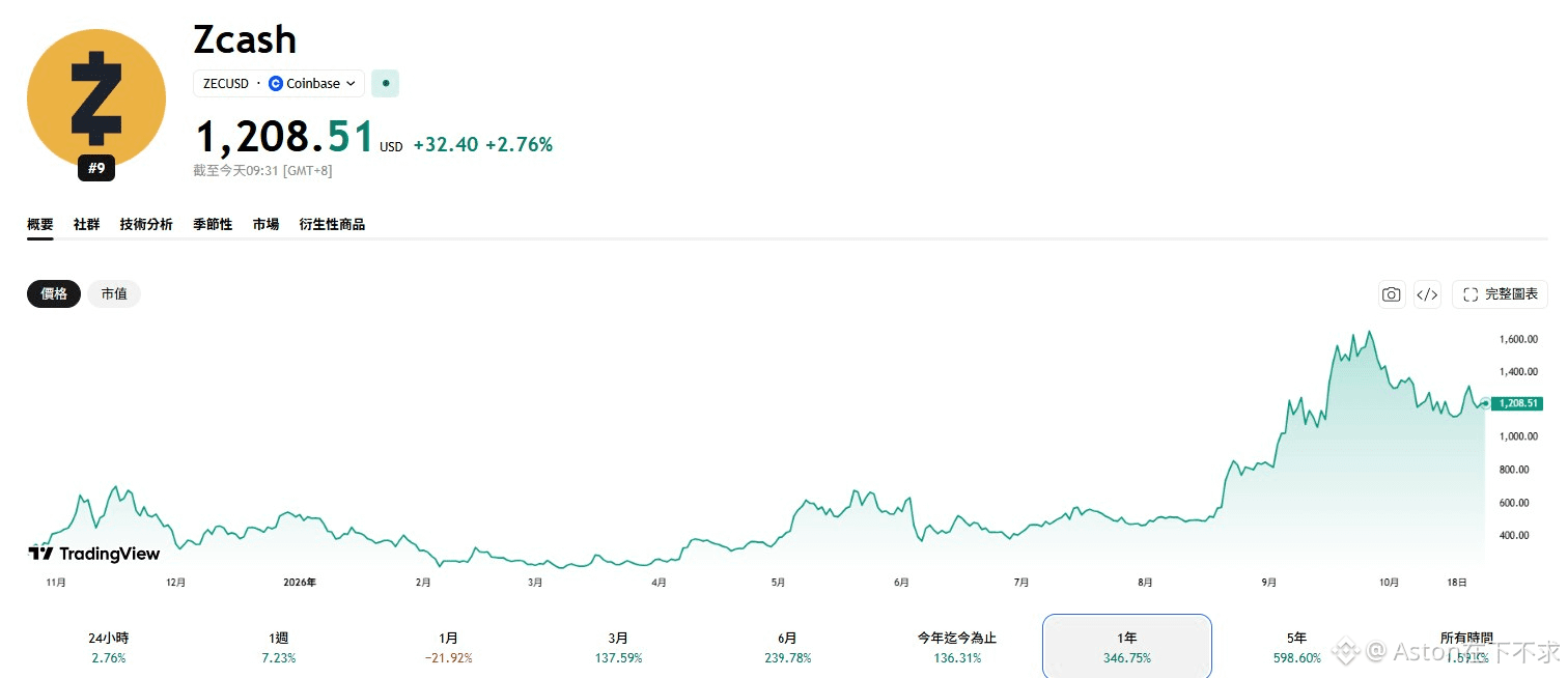
296
·
--
Verified
Article
iPhone Duo Unboxing: Heavier Than Samsung, No Dedicated Telephoto Camera$SOXX $SMH $SOXL #苹果 #X #三星
Apple launches its first foldable-screen smartphone, the iPhone Duo, which supports running two full apps side by side and using them independently on the desktop. After unboxing and testing it, tech YouTuber “The Tech Chap” said the iPhone Duo excels at multitasking and battery life, but its high price, heavy body, and lack of pro-grade camera features mean it isn't his top recommendation.
What's special about the split-screen browsing feature?
The iPhone Duo features a passport-like folding design and a mirror-polished titanium frame, with IP68-rated water and dust resistance. Its inner screen uses a nano-texture display to reduce glare and fingerprints, but can look a little duller than the glossy outer screen in certain lighting.
iPhone Duo Unboxing: Heavier Than Samsung, No Dedicated Telephoto Camera
$SOXX $SMH $SOXL #苹果 #X #三星
Apple launches its first foldable-screen smartphone, the iPhone Duo, which supports running two full apps side by side and using them independently on the desktop. After unboxing and testing it, tech YouTuber “The Tech Chap” said the iPhone Duo excels at multitasking and battery life, but its high price, heavy body, and lack of pro-grade camera features mean it isn't his top recommendation.
What's special about the split-screen browsing feature?
The iPhone Duo features a passport-like folding design and a mirror-polished titanium frame, with IP68-rated water and dust resistance. Its inner screen uses a nano-texture display to reduce glare and fingerprints, but can look a little duller than the glossy outer screen in certain lighting.
Apple launches its first foldable-screen smartphone, the iPhone Duo, which supports running two full apps side by side and using them independently on the desktop. After unboxing and testing it, tech YouTuber “The Tech Chap” said the iPhone Duo excels at multitasking and battery life, but its high price, heavy body, and lack of pro-grade camera features mean it isn't his top recommendation.
What's special about the split-screen browsing feature?
The iPhone Duo features a passport-like folding design and a mirror-polished titanium frame, with IP68-rated water and dust resistance. Its inner screen uses a nano-texture display to reduce glare and fingerprints, but can look a little duller than the glossy outer screen in certain lighting.
619
·
--
$BTC $ETH $SOL
Bitcoin briefly falls below $80,000; $346 million in long positions liquidated in 24 hours
According to CoinGecko data, Bitcoin briefly fell to $79,941 at around 10:30 p.m. Taiwan time on October 24, dropping below the $80,000 mark. As of 10:45 p.m., Bitcoin was trading at $80,157, down about 1.8% over 24 hours. Its 24-hour high was $81,742, recorded at 10:55 p.m. on October 23. Other major cryptocurrencies also weakened. At the same time, Ethereum was trading at $2,343, down about 2.6% over 24 hours, while Solana was at $100.54, down about 3.8%.
$480 million liquidated in 24 hours, with 70% in long positions
According to CoinGlass data, as of 10:30 p.m. Taiwan time, 195,432 traders had been liquidated across the market over the previous 24 hours, for a total of $480 million. Of that amount, $346 million was in long positions and $134 million in short positions, meaning long positions accounted for 72%. The largest single liquidation was a $4.77 million long position in an Ethereum perpetual contract on Binance. Looking only at the previous 12 hours, liquidations totaled $64 million, including $51.05 million in long positions.
Spot ETFs see net outflows for two consecutive trading days
U.S. spot Bitcoin ETFs have recorded net outflows over the past two trading days. According to Farside Investors data, the ETFs saw combined net outflows of $636 million on October 22, Eastern Time, including $254 million from BlackRock’s IBIT. On October 23, they recorded another $138 million in net outflows, with $110 million flowing out of IBIT. Before that, on October 21, the ETFs had seen net inflows of $525 million.
On October 22, it was reported that Bitcoin ETFs had seen $1.07 billion in inflows over three days, yet the price had retreated before reaching $85,000. So far, there has been no single clear trigger for this latest drop below $80,000.
This article, “Bitcoin briefly falls below $80,000; $346 million in long positions liquidated in 24 hours,” first appeared on .
$BTC $ETH $SOL
Bitcoin briefly falls below $80,000; $346 million in long positions liquidated in 24 hours
According to CoinGecko data, Bitcoin briefly fell to $79,941 at around 10:30 p.m. Taiwan time on October 24, dropping below the $80,000 mark. As of 10:45 p.m., Bitcoin was trading at $80,157, down about 1.8% over 24 hours. Its 24-hour high was $81,742, recorded at 10:55 p.m. on October 23. Other major cryptocurrencies also weakened. At the same time, Ethereum was trading at $2,343, down about 2.6% over 24 hours, while Solana was at $100.54, down about 3.8%.
$480 million liquidated in 24 hours, with 70% in long positions
According to CoinGlass data, as of 10:30 p.m. Taiwan time, 195,432 traders had been liquidated across the market over the previous 24 hours, for a total of $480 million. Of that amount, $346 million was in long positions and $134 million in short positions, meaning long positions accounted for 72%. The largest single liquidation was a $4.77 million long position in an Ethereum perpetual contract on Binance. Looking only at the previous 12 hours, liquidations totaled $64 million, including $51.05 million in long positions.
Spot ETFs see net outflows for two consecutive trading days
U.S. spot Bitcoin ETFs have recorded net outflows over the past two trading days. According to Farside Investors data, the ETFs saw combined net outflows of $636 million on October 22, Eastern Time, including $254 million from BlackRock’s IBIT. On October 23, they recorded another $138 million in net outflows, with $110 million flowing out of IBIT. Before that, on October 21, the ETFs had seen net inflows of $525 million.
On October 22, it was reported that Bitcoin ETFs had seen $1.07 billion in inflows over three days, yet the price had retreated before reaching $85,000. So far, there has been no single clear trigger for this latest drop below $80,000.
This article, “Bitcoin briefly falls below $80,000; $346 million in long positions liquidated in 24 hours,” first appeared on .
Bitcoin briefly falls below $80,000; $346 million in long positions liquidated in 24 hours
According to CoinGecko data, Bitcoin briefly fell to $79,941 at around 10:30 p.m. Taiwan time on October 24, dropping below the $80,000 mark. As of 10:45 p.m., Bitcoin was trading at $80,157, down about 1.8% over 24 hours. Its 24-hour high was $81,742, recorded at 10:55 p.m. on October 23. Other major cryptocurrencies also weakened. At the same time, Ethereum was trading at $2,343, down about 2.6% over 24 hours, while Solana was at $100.54, down about 3.8%.
$480 million liquidated in 24 hours, with 70% in long positions
According to CoinGlass data, as of 10:30 p.m. Taiwan time, 195,432 traders had been liquidated across the market over the previous 24 hours, for a total of $480 million. Of that amount, $346 million was in long positions and $134 million in short positions, meaning long positions accounted for 72%. The largest single liquidation was a $4.77 million long position in an Ethereum perpetual contract on Binance. Looking only at the previous 12 hours, liquidations totaled $64 million, including $51.05 million in long positions.
Spot ETFs see net outflows for two consecutive trading days
U.S. spot Bitcoin ETFs have recorded net outflows over the past two trading days. According to Farside Investors data, the ETFs saw combined net outflows of $636 million on October 22, Eastern Time, including $254 million from BlackRock’s IBIT. On October 23, they recorded another $138 million in net outflows, with $110 million flowing out of IBIT. Before that, on October 21, the ETFs had seen net inflows of $525 million.
On October 22, it was reported that Bitcoin ETFs had seen $1.07 billion in inflows over three days, yet the price had retreated before reaching $85,000. So far, there has been no single clear trigger for this latest drop below $80,000.
This article, “Bitcoin briefly falls below $80,000; $346 million in long positions liquidated in 24 hours,” first appeared on .


1
148
·
--

Article
Bitcoin briefly falls below $80,000, with $346 million in long positions liquidated over 24 hours$BTC $ETH $SOL #比特幣本周回落至約84600美元 #ETF #Bitcoin
According to CoinGecko data, Bitcoin briefly fell to $79,941 at around 10:30 p.m. Taiwan time on October 24, dropping below the $80,000 mark. As of 10:45 p.m., Bitcoin was trading at $80,157, down about 1.8% over 24 hours. Its high over the past 24 hours was $81,742, recorded at 10:55 p.m. on October 23.
Other major cryptocurrencies also weakened. At the same time, Ethereum was trading at $2,343, down about 2.6% over 24 hours, while Solana was at $100.54, down about 3.8%.
$480 million in liquidations over 24 hours, 70% of them long positions
Bitcoin briefly falls below $80,000, with $346 million in long positions liquidated over 24 hours
$BTC $ETH $SOL #比特幣本周回落至約84600美元 #ETF #Bitcoin
According to CoinGecko data, Bitcoin briefly fell to $79,941 at around 10:30 p.m. Taiwan time on October 24, dropping below the $80,000 mark. As of 10:45 p.m., Bitcoin was trading at $80,157, down about 1.8% over 24 hours. Its high over the past 24 hours was $81,742, recorded at 10:55 p.m. on October 23.
Other major cryptocurrencies also weakened. At the same time, Ethereum was trading at $2,343, down about 2.6% over 24 hours, while Solana was at $100.54, down about 3.8%.
$480 million in liquidations over 24 hours, 70% of them long positions
According to CoinGecko data, Bitcoin briefly fell to $79,941 at around 10:30 p.m. Taiwan time on October 24, dropping below the $80,000 mark. As of 10:45 p.m., Bitcoin was trading at $80,157, down about 1.8% over 24 hours. Its high over the past 24 hours was $81,742, recorded at 10:55 p.m. on October 23.
Other major cryptocurrencies also weakened. At the same time, Ethereum was trading at $2,343, down about 2.6% over 24 hours, while Solana was at $100.54, down about 3.8%.
$480 million in liquidations over 24 hours, 70% of them long positions
672
·
--
Partly True
U.S. Stocks Earnings Preview and Conference Call Guide for This WeekToday is October 24, 2026. This week, U.S. stocks enter a busy earnings season for tech giants and industrial leaders. Here is a roundup of earnings updates from the 100 largest companies by market capitalization with the greatest potential impact:
### 📅 Key Earnings Releases and Conference Call Schedule This Week
| U.S. Date | Company/Ticker | Session | Conference Call (Taiwan Time) |
| :--- | :--- | :--- | :--- |
| 10/27 (Tue) | Alphabet (GOOGL) | After market close | 10/28 05:00 |
| 10/28 (Wed) | Microsoft ($MSFT) | After market close | 10/29 05:30 |
| 10/29 (Thu) | Meta Platforms ($META) | After market close | 10/30 05:00 |
U.S. Stocks Earnings Preview and Conference Call Guide for This Week
Today is October 24, 2026. This week, U.S. stocks enter a busy earnings season for tech giants and industrial leaders. Here is a roundup of earnings updates from the 100 largest companies by market capitalization with the greatest potential impact:
### 📅 Key Earnings Releases and Conference Call Schedule This Week
| U.S. Date | Company/Ticker | Session | Conference Call (Taiwan Time) |
| :--- | :--- | :--- | :--- |
| 10/27 (Tue) | Alphabet (GOOGL) | After market close | 10/28 05:00 |
| 10/28 (Wed) | Microsoft ($MSFT ) | After market close | 10/29 05:30 |
| 10/29 (Thu) | Meta Platforms ($META ) | After market close | 10/30 05:00 |
### 📅 Key Earnings Releases and Conference Call Schedule This Week
| U.S. Date | Company/Ticker | Session | Conference Call (Taiwan Time) |
| :--- | :--- | :--- | :--- |
| 10/27 (Tue) | Alphabet (GOOGL) | After market close | 10/28 05:00 |
| 10/28 (Wed) | Microsoft ($MSFT ) | After market close | 10/29 05:30 |
| 10/29 (Thu) | Meta Platforms ($META ) | After market close | 10/30 05:00 |
2
6.5k
·
--
$TSLA $SPCX
SpaceX quarterly report reveals: Tesla merger would also require approval from controlling shareholder Musk
SpaceX’s third-quarter report (10-Q), filed with the U.S. Securities and Exchange Commission on October 22, states that a merger with Tesla would require approval not only from SpaceX’s special committee and board of directors, but also from its “controlling shareholder.” According to SpaceX’s June IPO prospectus, that controlling shareholder is CEO Elon Musk.
The report says that during its earnings call on October 20, SpaceX announced that its board had formed a special committee to evaluate the possibility of a merger with Tesla. Tesla’s board also formed a special committee. SpaceX’s special committee has not yet made any decisions. “Any potential merger would require further approval from our special committee, board of directors, and controlling shareholder,” the report states. SpaceX also said there is no guarantee that the two sides will reach an agreement or complete a transaction, and that the special committee may decide not to recommend one.
Musk holds more than 80% of SpaceX’s voting power
According to the prospectus, based on an IPO price of $135 per share, Musk will hold approximately 82.4% of the voting power in SpaceX after its IPO through his Class A and Class B common stock. Class B shareholders can independently elect 51% of the directors. Musk holds a majority of the Class B shares, allowing him to elect and remove Class B directors. As long as he holds more than 50% of the voting power, he can control the board’s composition and the outcome of matters requiring a shareholder vote. As a result, SpaceX qualifies as a “controlled company” under Nasdaq rules and may be exempt from requirements such as having a majority-independent board.
Tesla’s quarterly report, filed the same day, states that its board formed a special committee of disinterested directors to study ways to deepen its relationship with SpaceX, potentially including a merger. Tesla said there is no guarantee that a transaction will be completed, and that it would require a favorable recommendation from the special committee and the necessary shareholder approvals after an agreement is reached. Tesla’s filing did not mention approval from a “controlling shareholder” as a condition.
Tesla purchases $480 million from SpaceX in the first three quarters; Tesla holds an equity stake in SpaceX
The related-party transactions note in SpaceX’s quarterly report shows that SpaceX purchased $480 million worth of Megapack energy storage products from Tesla in the first three quarters of this year, including $151 million in the third quarter. Tesla also holds an equity stake in SpaceX. Measured at fair value, Tesla recognized $863 million in unrealized gains in the first three quarters. Tesla explained in its quarterly report that it is presumed to have significant influence over SpaceX because both companies are led by the same CEO.
Earlier reports said Barclays had estimated that the two companies might announce a merger by December.
This article, “SpaceX quarterly report reveals: Tesla merger would also require approval from controlling shareholder Musk,” first appeared at .
$TSLA $SPCX
SpaceX quarterly report reveals: Tesla merger would also require approval from controlling shareholder Musk
SpaceX’s third-quarter report (10-Q), filed with the U.S. Securities and Exchange Commission on October 22, states that a merger with Tesla would require approval not only from SpaceX’s special committee and board of directors, but also from its “controlling shareholder.” According to SpaceX’s June IPO prospectus, that controlling shareholder is CEO Elon Musk.
The report says that during its earnings call on October 20, SpaceX announced that its board had formed a special committee to evaluate the possibility of a merger with Tesla. Tesla’s board also formed a special committee. SpaceX’s special committee has not yet made any decisions. “Any potential merger would require further approval from our special committee, board of directors, and controlling shareholder,” the report states. SpaceX also said there is no guarantee that the two sides will reach an agreement or complete a transaction, and that the special committee may decide not to recommend one.
Musk holds more than 80% of SpaceX’s voting power
According to the prospectus, based on an IPO price of $135 per share, Musk will hold approximately 82.4% of the voting power in SpaceX after its IPO through his Class A and Class B common stock. Class B shareholders can independently elect 51% of the directors. Musk holds a majority of the Class B shares, allowing him to elect and remove Class B directors. As long as he holds more than 50% of the voting power, he can control the board’s composition and the outcome of matters requiring a shareholder vote. As a result, SpaceX qualifies as a “controlled company” under Nasdaq rules and may be exempt from requirements such as having a majority-independent board.
Tesla’s quarterly report, filed the same day, states that its board formed a special committee of disinterested directors to study ways to deepen its relationship with SpaceX, potentially including a merger. Tesla said there is no guarantee that a transaction will be completed, and that it would require a favorable recommendation from the special committee and the necessary shareholder approvals after an agreement is reached. Tesla’s filing did not mention approval from a “controlling shareholder” as a condition.
Tesla purchases $480 million from SpaceX in the first three quarters; Tesla holds an equity stake in SpaceX
The related-party transactions note in SpaceX’s quarterly report shows that SpaceX purchased $480 million worth of Megapack energy storage products from Tesla in the first three quarters of this year, including $151 million in the third quarter. Tesla also holds an equity stake in SpaceX. Measured at fair value, Tesla recognized $863 million in unrealized gains in the first three quarters. Tesla explained in its quarterly report that it is presumed to have significant influence over SpaceX because both companies are led by the same CEO.
Earlier reports said Barclays had estimated that the two companies might announce a merger by December.
This article, “SpaceX quarterly report reveals: Tesla merger would also require approval from controlling shareholder Musk,” first appeared at .
SpaceX quarterly report reveals: Tesla merger would also require approval from controlling shareholder Musk
SpaceX’s third-quarter report (10-Q), filed with the U.S. Securities and Exchange Commission on October 22, states that a merger with Tesla would require approval not only from SpaceX’s special committee and board of directors, but also from its “controlling shareholder.” According to SpaceX’s June IPO prospectus, that controlling shareholder is CEO Elon Musk.
The report says that during its earnings call on October 20, SpaceX announced that its board had formed a special committee to evaluate the possibility of a merger with Tesla. Tesla’s board also formed a special committee. SpaceX’s special committee has not yet made any decisions. “Any potential merger would require further approval from our special committee, board of directors, and controlling shareholder,” the report states. SpaceX also said there is no guarantee that the two sides will reach an agreement or complete a transaction, and that the special committee may decide not to recommend one.
Musk holds more than 80% of SpaceX’s voting power
According to the prospectus, based on an IPO price of $135 per share, Musk will hold approximately 82.4% of the voting power in SpaceX after its IPO through his Class A and Class B common stock. Class B shareholders can independently elect 51% of the directors. Musk holds a majority of the Class B shares, allowing him to elect and remove Class B directors. As long as he holds more than 50% of the voting power, he can control the board’s composition and the outcome of matters requiring a shareholder vote. As a result, SpaceX qualifies as a “controlled company” under Nasdaq rules and may be exempt from requirements such as having a majority-independent board.
Tesla’s quarterly report, filed the same day, states that its board formed a special committee of disinterested directors to study ways to deepen its relationship with SpaceX, potentially including a merger. Tesla said there is no guarantee that a transaction will be completed, and that it would require a favorable recommendation from the special committee and the necessary shareholder approvals after an agreement is reached. Tesla’s filing did not mention approval from a “controlling shareholder” as a condition.
Tesla purchases $480 million from SpaceX in the first three quarters; Tesla holds an equity stake in SpaceX
The related-party transactions note in SpaceX’s quarterly report shows that SpaceX purchased $480 million worth of Megapack energy storage products from Tesla in the first three quarters of this year, including $151 million in the third quarter. Tesla also holds an equity stake in SpaceX. Measured at fair value, Tesla recognized $863 million in unrealized gains in the first three quarters. Tesla explained in its quarterly report that it is presumed to have significant influence over SpaceX because both companies are led by the same CEO.
Earlier reports said Barclays had estimated that the two companies might announce a merger by December.
This article, “SpaceX quarterly report reveals: Tesla merger would also require approval from controlling shareholder Musk,” first appeared at .


1
327
Log in to explore more content
Join global crypto users on Binance Square
⚡️ Get latest and useful information about crypto.
💬 Trusted by the world’s largest crypto exchange.
👍 Discover real insights from verified creators.
Email / Phone number
Trending Topics
BinancePick
2.5M views
137,927 Discussing
Join #EarningsSeason: Predict Earnings on Binance Pick, Share Your Take on Binance Square!
Binance Square Official
·400 Likes
·337.1k views
EarningsSeason
4.9M views
23,915 Discussing
ElectrumWalletBugLetRogueServersStealFunds
2,613 views
137 Discussing