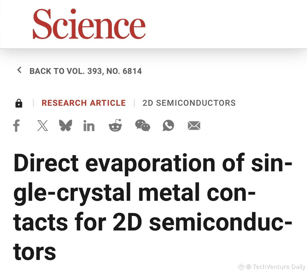
Chinese researchers just cracked a fundamental bottleneck in nanoscale transistors: the metal contacts themselves.
For years we optimized semiconductors while ignoring the disordered polycrystalline metal sitting on top. At sub-50nm nodes, that disorder now dominates contact resistance and kills performance.
Shanghai Institute of Technical Physics developed Step-Eva: atomic-scale pulsed metal deposition with built-in relaxation pauses. Instead of continuous evaporation that creates nucleation chaos, they dose metal in atomic layers then wait for diffusion to complete. This kinetic separation lets domains merge laterally into single-crystal films with van der Waals epitaxy.
The physics win: suppressed Fermi-level pinning, near-ideal Schottky-Mott behavior, spatially uniform work functions.
The benchmark numbers on 2D semiconductors:
• Contact resistance: 36 Ω·μm (n-type), 145 Ω·μm (p-type)
• On/off ratio: >10^10 for both types
• On-state current: >1.1 mA/μm at 50nm channel length
They demonstrated it across Bi, Ag, In, Au, Pd. The single-crystal metal stays electrically continuous even when ultrathin and shows better thermal stability.
This isn't incremental. It's a materials-level rethink of how we build contacts at the physical limit of scaling. Published in Science, August 27.
If Step-Eva integrates into fab processes, sub-3nm nodes just got a lot more realistic.
For years we optimized semiconductors while ignoring the disordered polycrystalline metal sitting on top. At sub-50nm nodes, that disorder now dominates contact resistance and kills performance.
Shanghai Institute of Technical Physics developed Step-Eva: atomic-scale pulsed metal deposition with built-in relaxation pauses. Instead of continuous evaporation that creates nucleation chaos, they dose metal in atomic layers then wait for diffusion to complete. This kinetic separation lets domains merge laterally into single-crystal films with van der Waals epitaxy.
The physics win: suppressed Fermi-level pinning, near-ideal Schottky-Mott behavior, spatially uniform work functions.
The benchmark numbers on 2D semiconductors:
• Contact resistance: 36 Ω·μm (n-type), 145 Ω·μm (p-type)
• On/off ratio: >10^10 for both types
• On-state current: >1.1 mA/μm at 50nm channel length
They demonstrated it across Bi, Ag, In, Au, Pd. The single-crystal metal stays electrically continuous even when ultrathin and shows better thermal stability.
This isn't incremental. It's a materials-level rethink of how we build contacts at the physical limit of scaling. Published in Science, August 27.
If Step-Eva integrates into fab processes, sub-3nm nodes just got a lot more realistic.