
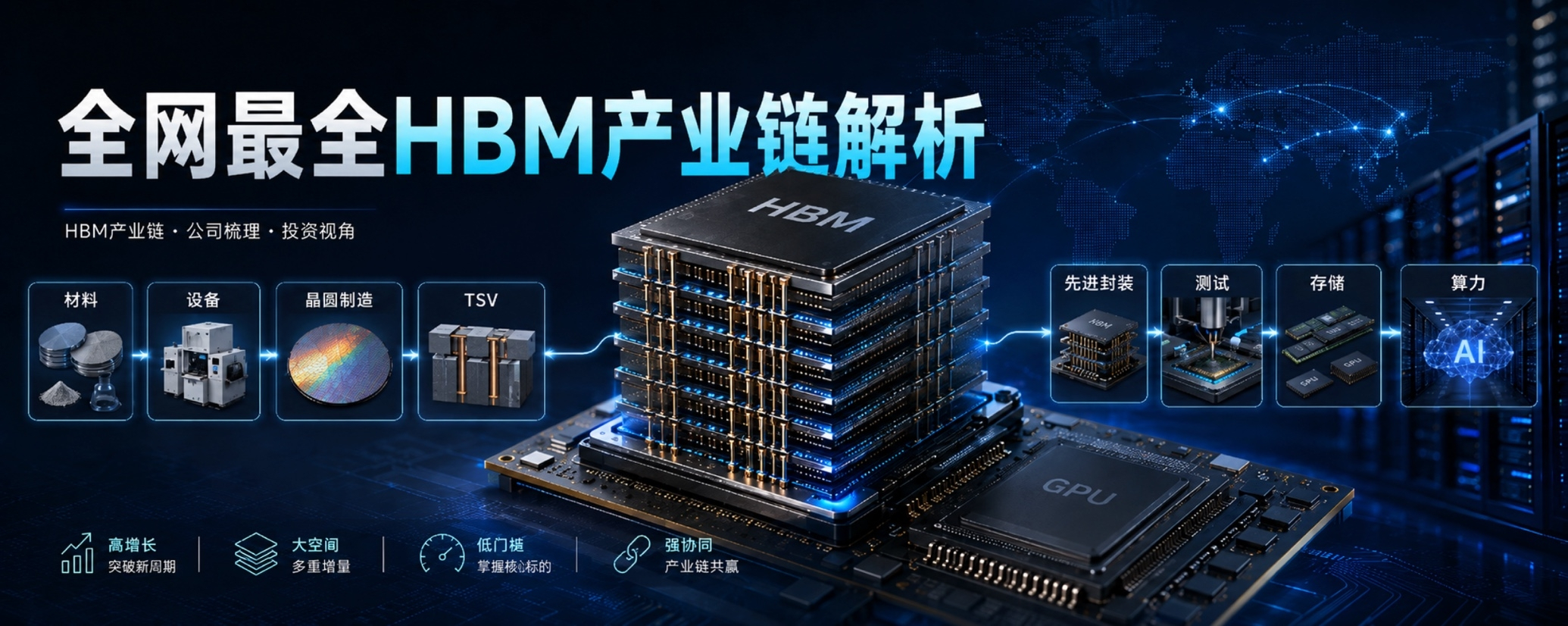

After browsing around, I noticed that there are only calls for trades and shared profits; no one is clearly explaining the entire HBM supply chain. Understanding the supply chain is crucial to know what to buy and what to avoid. Today, let me shed some light on this.
What is HBM?
HBM, or High Bandwidth Memory, utilizes Through-Silicon Vias (TSV) to vertically stack multiple layers of DRAM, achieving extreme memory bandwidth and low latency, providing massive data throughput capabilities for AI GPUs like NVIDIA, breaking through the traditional memory 'wall' bottleneck.
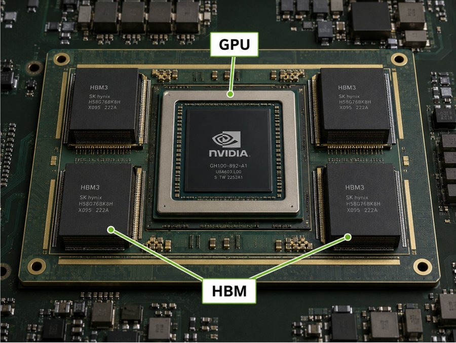
What is the core technology behind HBM?
In simple terms, HBM stacks multiple layers of DRAM chips vertically using stacking technology. The key process here is TSV (Through-Silicon Via); this involves not just laser drilling but etching gases that continuously corrode the silicon wafer to create holes and inject copper; then, a layer of tin (bumps) is applied on top of the injected copper, allowing multiple bare chips to be stacked together.
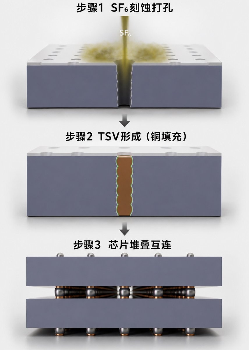
In this process, the most important parts are four:
HBM design and manufacturing: made by SK Hynix, Micron, and Samsung Electronics themselves
TSV via-hole equipment: Applied Materials $AMAT and Lam Research $LRCX monopolize it
Etching / deposition / polishing materials: Integre / Integ?
$ENTG
HBM testing probe cards: FormFactor $FORM (a deeply cooperating partner with Hynix)
But if it’s only stacking, then besides the micro-bump connections everything is suspended and therefore quite fragile. To strengthen and for heat dissipation, currently the big three vendors have two approaches:
SK Hynix first stacks everything as a whole, then puts the entire HBM into a grinding mold and pours liquid epoxy resin into it to fill the gaps. Then heating and applying pressure solidify the epoxy resin.
Samsung and Micron, on the other hand, add a layer of high-molecular thin film between the two chip layers. When heating and applying pressure, the thin film at the micro-bump spots melts to complete the bonding, and after cooling the thin film solidifies. Then this process is repeated over and over to stack upward.
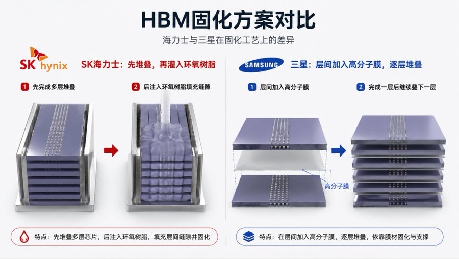
For these two approaches, SK Hynix is the best, because during micro-bump bonding there’s nothing else that interferes, so manufacturing speed and yield will be much better.
For heat dissipation, SK Hynix also mixes high-thermal-conductivity particles into the epoxy resin—essentially turning the epoxy resin into something similar to thermal grease. SK Hynix’s heat-dissipation efficiency is twice that of Samsung. So how can Hynix’s market share reach 50%?
So if it’s a Hynix ADR, just use the mu you have on hand directly to switch to Hynix.
HBM integration and packaging — CoWos
After HBM is manufactured, the next step is the work of connecting it to the GPU. Traditionally, connections between circuit boards and chips are made by etching circuits on the PCB. But the communication wiring between HBM and the GPU is extremely complex. The circuit density achievable with ordinary PCBs simply can’t match that. So TSMC
$TSM
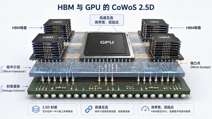
Then they introduced a 2.5D packaging method called CoWos.
The principle is to directly use a lithography machine to pattern the circuit that connects HBM and the GPU onto a large silicon wafer (the spacing between lines can be as small as 0.8 to 2μm). Then the two types of chips are directly soldered together. This can achieve both high bandwidth and low latency. NVIDIA’s H100 and B200 use this approach.
What about CoPos?
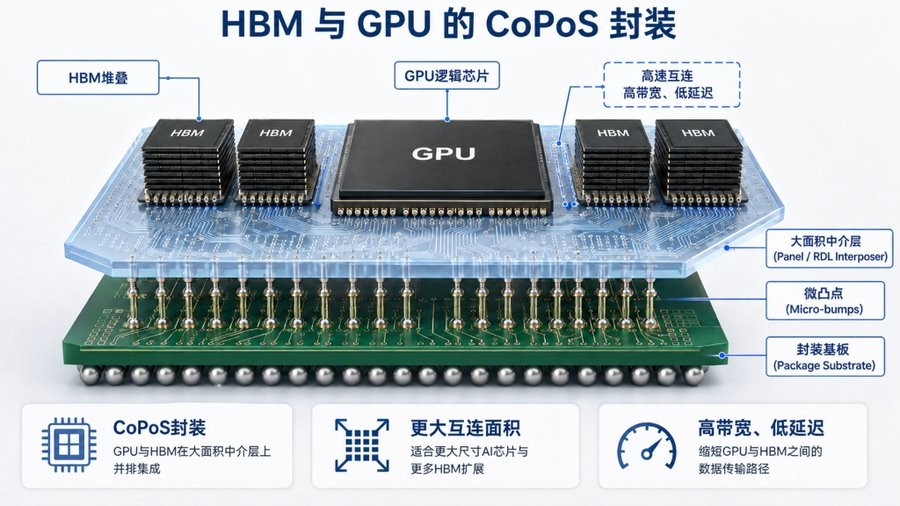
Simply put, silicon wafer panels are currently expensive and they’re also circular. Most mainstream chips, however, are square. Cutting circular silicon wafers is very wasteful. So people have proposed arranging chips on a square “panel RDL layer” to replace the original circular silicon interposer. This strengthens how circuits are laid out for interconnection among different conductive layers and materials. With the introduction of new materials such as glass or sapphire, the square size can support packaging of multiple chips, integrating chips of different sizes. It also supports larger masks and mitigates the warping problem that becomes more obvious as chips get larger.
But the interconnect density is relatively weaker right now. Panel-level tools and yields are still being developed; they’re still in pilot production / ramp-up stage, unlike CoWoS, which is already fully mature and in mass production.
These advanced packaging technologies mainly rely on TSMC $TSM and $AMKR.
, on June 16 these two companies also signed 10-year long-term contracts, which proves that this capacity is indeed insufficient.
CoWoS is the current mainstay (2.5D). CoPoS plus a glass substrate is the next-generation direction for large-scale sizes. $TSM through the 3DFabric platform, they can be combined flexibly to comprehensively cover packaging needs from AI to mobile devices.
At the moment, the direction of TSV via-hole equipment, HBM testing, and CoWoS still has a lot of opportunity.
The above is only personal analysis and does not constitute investment advice. DYOR~