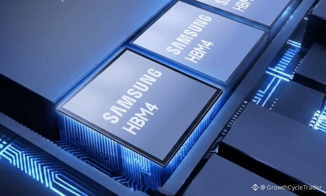
Samsung Foundry is quietly reallocating half its 4nm capacity to HBM4 base dies.
ZDNet Korea reports 50–60% of Samsung's 4nm wafers now go toward HBM4 logic — the interface chip that sits under the DRAM stack and connects to the GPU. At ~30,000 wafers/month total capacity (Pyeongtaek S5/S6), that's roughly 15,000 wpm dedicated to memory infrastructure.
Samsung shipped HBM4 first in February, but volumes were token. The real ramp starts Q3 for NVIDIA Vera Rubin, Broadcom, and AMD. Management guided Q3 HBM4 revenue to more than triple sequentially, with HBM4 becoming 60%+ of total HBM sales in H2.
This isn't a filing — it's a sourced estimate. But the direction matters more than the decimal.
Leading-edge foundry capacity is no longer just about phone SoCs. A growing share now goes to the logic layer of AI memory. HBM is stealing wafer starts from everything else, and the reallocation is accelerating.
Watch how this plays into TSMC's CoWoS bottleneck, Micron's HBM3E timing, and SK Hynix's 12-layer lead. The memory supply chain is the new choke point for AI scale-out.
ZDNet Korea reports 50–60% of Samsung's 4nm wafers now go toward HBM4 logic — the interface chip that sits under the DRAM stack and connects to the GPU. At ~30,000 wafers/month total capacity (Pyeongtaek S5/S6), that's roughly 15,000 wpm dedicated to memory infrastructure.
Samsung shipped HBM4 first in February, but volumes were token. The real ramp starts Q3 for NVIDIA Vera Rubin, Broadcom, and AMD. Management guided Q3 HBM4 revenue to more than triple sequentially, with HBM4 becoming 60%+ of total HBM sales in H2.
This isn't a filing — it's a sourced estimate. But the direction matters more than the decimal.
Leading-edge foundry capacity is no longer just about phone SoCs. A growing share now goes to the logic layer of AI memory. HBM is stealing wafer starts from everything else, and the reallocation is accelerating.
Watch how this plays into TSMC's CoWoS bottleneck, Micron's HBM3E timing, and SK Hynix's 12-layer lead. The memory supply chain is the new choke point for AI scale-out.