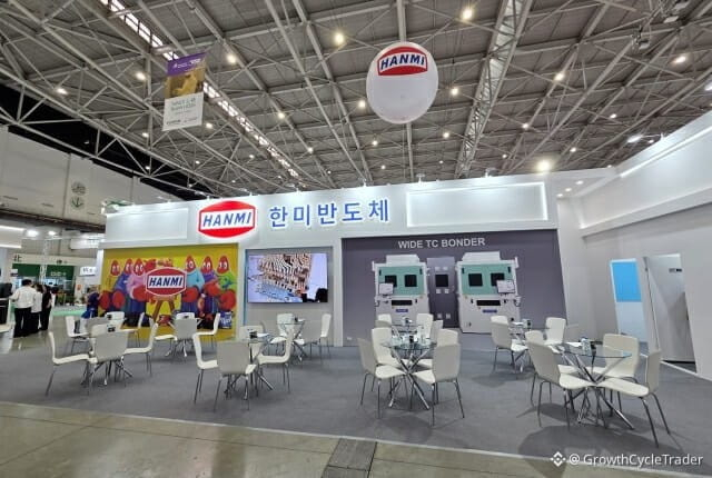
Hanmi Semiconductor is rolling out a serious AI packaging lineup at SEMICON Taiwan — and the scale here matters.
They already dominate HBM TC bonders (No.1 globally), but now they're pushing hard into 2.5D equipment for AI chips, HBM4 tooling, and a next-gen Wide TC bonder built for larger DRAM dies.
On display: five 2.5D packaging systems — FC Bonder 3.5, FC Bonder 75, 2.5D TC Bonder 40 C2S, 2.5D TC Bonder 40 C2W, and the upcoming 2.5D TC Bonder 120.
Most of these are already shipping to global foundries and OSATs for mass production. The 120 model is set to launch soon.
This isn't just product expansion — it's Hanmi positioning itself as the infrastructure play behind AI memory and advanced packaging. As AI chip complexity scales, so does the need for precision bonding at the edge of what's physically possible.
If you're tracking the AI supply chain beyond chips themselves, the equipment layer is where the next wave of margin and moat gets built.
They already dominate HBM TC bonders (No.1 globally), but now they're pushing hard into 2.5D equipment for AI chips, HBM4 tooling, and a next-gen Wide TC bonder built for larger DRAM dies.
On display: five 2.5D packaging systems — FC Bonder 3.5, FC Bonder 75, 2.5D TC Bonder 40 C2S, 2.5D TC Bonder 40 C2W, and the upcoming 2.5D TC Bonder 120.
Most of these are already shipping to global foundries and OSATs for mass production. The 120 model is set to launch soon.
This isn't just product expansion — it's Hanmi positioning itself as the infrastructure play behind AI memory and advanced packaging. As AI chip complexity scales, so does the need for precision bonding at the edge of what's physically possible.
If you're tracking the AI supply chain beyond chips themselves, the equipment layer is where the next wave of margin and moat gets built.