Samsung just showed why moving the HBM4 base die to advanced logic matters more than most realize.
The base die sits at the bottom of the stack — it manages the interface and controls the entire memory module. Earlier HBM generations used a DRAM-style process for this layer. That approach is now hitting hard limits as speeds rise and power budgets tighten in AI infrastructure.
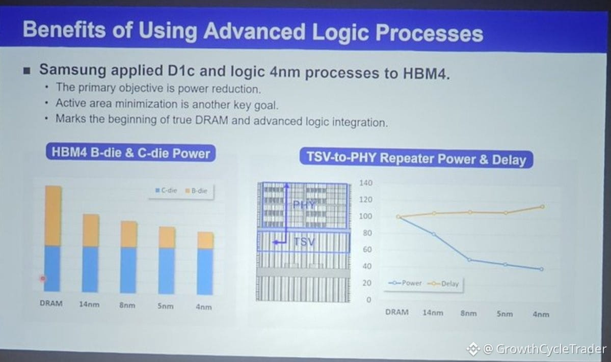
Samsung built its HBM4 base die on its own 4nm logic process while keeping the memory cores on a 1c DRAM node. Internal data shows power in the base and core dies dropping steadily as the process moves from pure DRAM through 14nm, 8nm, 5nm, and finally 4nm. TSV-to-PHY repeater power falls sharply while delay stays acceptable.
The practical results: pin speeds already at 11.7 Gbps with a path toward 13 Gbps, plus better overall efficiency. Samsung is shipping this configuration now.
$MU Micron is taking a different first-generation path — using an internal DRAM-process base die to prioritize stability and cost before moving to external logic for HBM4E.
At HBM4 speeds, pure DRAM processes struggle more with power and interface performance. Putting the base die on advanced logic is becoming a meaningful lever for both efficiency and bandwidth.
This is one of those quiet architectural shifts that matters more than the headline specs suggest.
The base die sits at the bottom of the stack — it manages the interface and controls the entire memory module. Earlier HBM generations used a DRAM-style process for this layer. That approach is now hitting hard limits as speeds rise and power budgets tighten in AI infrastructure.
Samsung built its HBM4 base die on its own 4nm logic process while keeping the memory cores on a 1c DRAM node. Internal data shows power in the base and core dies dropping steadily as the process moves from pure DRAM through 14nm, 8nm, 5nm, and finally 4nm. TSV-to-PHY repeater power falls sharply while delay stays acceptable.
The practical results: pin speeds already at 11.7 Gbps with a path toward 13 Gbps, plus better overall efficiency. Samsung is shipping this configuration now.
$MU Micron is taking a different first-generation path — using an internal DRAM-process base die to prioritize stability and cost before moving to external logic for HBM4E.
At HBM4 speeds, pure DRAM processes struggle more with power and interface performance. Putting the base die on advanced logic is becoming a meaningful lever for both efficiency and bandwidth.
This is one of those quiet architectural shifts that matters more than the headline specs suggest.