
Article reprint source: Chip Guest
Original source: Hard AI

Image source: Generated by Unbounded AI
In the past two days, there have been rumors that Nvidia has "taken advantage of a loophole" to break through US AI restrictions, launched "special models" for the Chinese market, and is preparing to continue selling high-performance GPUs to Chinese companies.
According to the latest media reports, NVIDIA is about to launch at least three new AI chips, including H20 SXM, PCIe L20 and PCIe L2, to replace the H100 that was previously restricted from export by the United States. All three chips are based on the Hopper GPU architecture, with a maximum theoretical performance of 296TFLOP (floating-point operations per second, also known as peak speed per second).
So, compared with H100, what are the performances of NVIDIA's three "special model" chips: H20, L20, and L2?
Theoretically, H100 is 6.68 times faster than H20. According to a recent blog post by analyst Dylan Petal, even if the actual utilization rate of H20 can reach 90%, its performance in an actual multi-card interconnection environment is still only close to 50% of H100.
Some media also said that the comprehensive computing power of H20 is only equivalent to 20% of H100, and due to the addition of HBM video memory and NVLink interconnect module, the computing power cost will increase significantly.
However, the advantages of H20 are also obvious. It is more than 20% faster than H100 in large language model (LLM) reasoning. The reason is that H20 is similar to the next-generation super AI chip H200 to be released next year in some aspects.
Nvidia has already sampled all three chips, with the H20 and L20 expected to launch in December this year, and the L2 in January next year. Product sampling will begin a month before launch.
 01
01
「H20 Vs. H100」
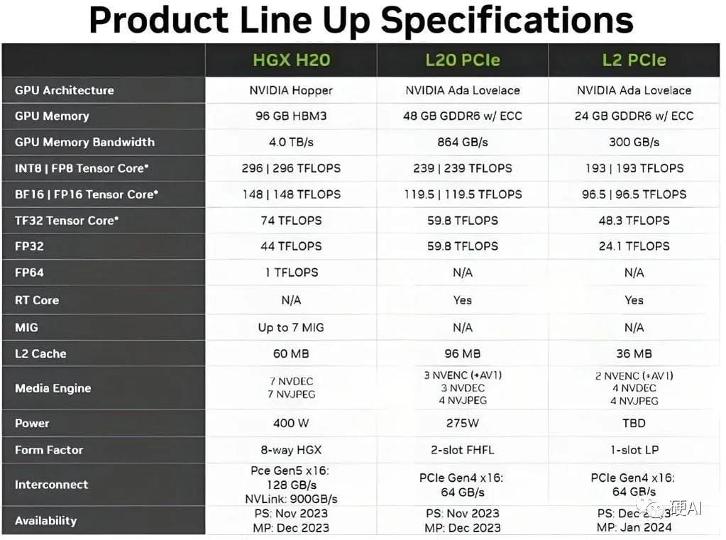
Let’s first look at the H100, which has 80GB of HBM3 memory, a memory bandwidth of 3.4Tb/s, a theoretical performance of 1979 TFLOPs, and a performance density (TFLOPs/Die size) of up to 19.4. It is the most powerful GPU in NVIDIA’s current product line.
H20 has 96GB HBM3 memory and a memory bandwidth of up to 4.0 Tb/s, both higher than H100, but its computing power is only 296 TFLOPs and its performance density is 2.9, which is far inferior to H100.
Theoretically, H100 is 6.68 times faster than H20. However, it is worth noting that this comparison is based on the floating point computing capabilities of FP16 Tensor Core (FP16 Tensor Core FLOPs), and sparse computing is enabled (greatly reducing the amount of calculations, so the speed will be significantly improved), so it does not fully reflect All its computing power.
In addition, the thermal design power consumption of this GPU is 400W, which is lower than the 700W of H100, and it can be configured with 8 GPUs in the HGX solution (NVIDIA's GPU server solution). It also retains the 900 GB/s NVLink high-speed interconnection function, and also provides 7-way MIG (Multi-Instance GPU) function.
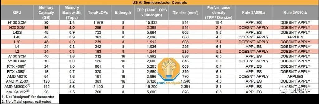
H100 SXM TF16(Sparsity)FLOPS = 1979
H20 SXM TF16(Sparsity)FLOPS = 296
According to Peta's LLM performance comparison model, the peak token/second of H20 at moderate batch size is 20% higher than that of H100, and the token-to-token latency at low batch size is 25% lower than that of H100. This is due to reducing the number of chips required for inference from 2 to 1. If 8-bit quantization is used, the LLAMA 70B model can run effectively on a single H20 instead of 2 H100s.
It is worth mentioning that although the computing power of H20 is only 296 TFLOPs, far less than the 1979 of H100, if the actual utilization rate of H20 is MFU (currently the MFU of H100 is only 38.1%), it means that H20 can actually run 270 TFLOPS, then the performance of H20 in an actual multi-card interconnection environment is close to 50% of H100.
From a traditional computing perspective, the H20 is a downgrade from the H100, but in terms of LLM reasoning, the H20 is actually more than 20% faster than the H100, because the H20 is similar in some ways to the H200 to be released next year. Note that the H200 is the successor to the H100, a super chip for complex AI and HPC workloads.
02
"L20 and L2 configurations are more streamlined"
Meanwhile, the L20 comes with 48 GB of memory and 239 TFLOPs of compute performance, while the L2 is configured with 24 GB of memory and 193 TFLOPs of compute performance.
L20 is based on L40 and L2 is based on L4, but these two chips are not commonly used in LLM inference and training.
Both the L20 and L2 use PCIe form factors, using PCIe specifications suitable for workstations and servers, and are more streamlined than higher-spec models such as the Hopper H800 and A800.
L40 TF16 (Sparsity) FLOPs = 362
L20 TF16 (Sparsity) FLOPs = 239
L4 TF16 (Sparsity) FLOPs = 242
L2 TF16 (Sparsity) FLOPs = 193